Continue to Site

Welcome to EDAboard.com

Welcome to our site! EDAboard.com is an international Electronics Discussion Forum focused on EDA software, circuits, schematics, books, theory, papers, asic, pld, 8051, DSP, Network, RF, Analog Design, PCB, Service Manuals... and a whole lot more! To participate you need to register. Registration is free. Click here to register now.

The Output Device of a Solid State Relay

Status
Not open for further replies.

PozFeedback

Newbie level 6
Newbie level 6
Joined
May 3, 2017
Messages
13
Helped
1
Reputation
2
Reaction score
1
Trophy points
3
Activity points
129
Hi,

The switching device of an SSR can be a transistor, an SCR, or a TRIAC. Apparently, a transistor can be used for both AC and DC SSRs. I don't understand how a transistor can both sink and source current in a transistor-based AC SSR?

Thanks in advance!
 

There are opto-MOSFET SSRs which are technically transistors but the drain-source connections are interchangeable so they will work on AC or DC. The majority of AC 'power' SSRs use a pair of back-to-back SCRs which works fine for AC but has no turn off mechanism for DC. In other words, they turn on and stay on until the current through them is broken elsewhere.

"sink and source" is not a sensible statement as they can only pass or block current. Nothing can be sourced from an internal circuit or sunk into it.

Brian.
 
Thanks for replying Brian!

Then a transistor-based AC SSR must use an MOS and it cannot be a BJT (due to the required symmetry in acting as a switch), am I right?

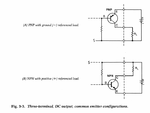
I have been recently studying "solid state relay handbook with applications". (Unfortunately, I did not find a newer reference to learn about SSRs). There, it is said that a 3-terminal transistor (as shown in the following figure) can be used to fully saturate the output BJT and achieve a switch with lower voltage drop.

3Terminal.png

But, with this configuration, how is it possible to turn the output device off? because now base is constantly connected to the supply via a resistor!

By the by, do you know a better reference for SSRs?

Thank you so much for your time.
 

I'm guessing the handbook is quite old. What it is showing is just a transistor acting as a switch which is quite in order but not what a conventional SSR does. The reason a relay is used in preference to the diagrams shown is because it provides a degree of isolation between the switch 'contacts' and the source of current energising it. In the diagrams the direct connection to the base and emitter to provide the activation implies current can also flow to or from the load directly.

Almost all SSR use optical technology to provide the isolation. The transistor/SCR/triac controlling the load side is driven from an internal optical sensor. That sensor is illiminated through an internal window that provides electrical isolation, typically of several KV. The light source is an LED which is powered from the control input signal. In darkness, the output devices turn off but when the LED is lit, the light passing through the window on to the sensor makes it 'leaky' and the current it passes turns the output device on.

Brian.
 

What it is showing is just a transistor acting as a switch which is quite in order but not what a conventional SSR does.
Brian.

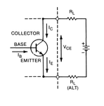
The diagrams show 'only the output stage' of a relay basically similar to today's technology. The book discusses two different configurations: two terminal connection as shown in the following diagram

2Terminal.png

and the 3-terminal configuration which was in my previous post. In the 3-terminal configuration, the base is somehow accessible from out of the chip and it is possible to apply a larger voltage to the BE-junction and fully saturate the transistor so that the collector-emitter voltage becomes 0.2 volt. (we achieve a switch with smaller voltage drop).

But I don't get how we can turn off the transistor in the 3-terminal configuration if its base is connected to a voltage from out of the SSR?
 

Hi,

I don't know much about this, frankly. The 4N35 optocoupler has the base pin available, maybe it's to bias it or something.

4n35 pinout.JPG

A DC (not for AC) SSR has this internal schematic in the datasheet.

cmx200d3 pinout.JPG

The schematics you post seem to be missing half the device or aren't really "relay" devices, surely - no isolation between control signal and output/switch. I might be wrong, but Renesas may have a little info about SSRs, or companies that make them on their websites, Crydom is one.
 
Your question doesn't relate to SSRs specifically, but to transistors used as switches in general.

To turn a transistor off, remove it's base current. That can be done by isolating the base current supply or by reducing the B-E voltage so it is low enough that the transistor ceases to pass any significant current. It's the B-E current source that decides whether the switch is on or off, if there is a resistor providing bias current (as shown in the diagrams) something with lower resistance that diverts the base current down a different route is what turns it off.

Brian.
 

Hi d123,

Thanks for replying.

The 4N35 optocoupler has the base pin available, maybe it's to bias it or something.

This was a good direction to follow, thanks!

I searched and found the following App. note:

http://www.soloelectronica.net/PDF/optoacopladores/app2.pdf

Only some of the opto-couplers have a lead for base connection. The above pdf explains that connecting the base to ground (or emitter), the device will act much faster but the collector current will be small. This case is suitable for high-speed applications. However, with the base left float, the collector current will be hundreds of times larger than the previous case (but at the cost of slower operation).

The schematics you post seem to be missing half the device or aren't really "relay" devices, surely - no isolation between control signal and output/switch.

These schematics are relays but they are only showing the output device (they are not showing the opto-coupler).

Renesas may have a little info about SSRs, or companies that make them on their websites, Crydom is one.

The diagrams that I have attached in my previous posts are taken from Crydom's handbook.
 
  • Like
Reactions: d123

    d123

    Points: 2
    Helpful Answer Positive Rating
Your question doesn't relate to SSRs specifically, but to transistors used as switches in general.

Thanks for replying Brian.

Sorry that I didn't completely and clearly explain my question. The schematics are the output device of a type of SSR. Because the book was discussing the switching device, it has omitted the opto-coupler. As explained in my previous post, according to my a-few-hour research, the base connection is available in some opt-couplers and allows us to face the trade-off between the device speed and its output current.

But, surprisingly, the book has mentioned that the base connection is made available to achieve a smaller voltage drop (when the output device is turned on)! Currently, I cannot make connection between what the book says and what is said in the appnote.
 

Unless some other unidentified circuit is actively driving the base connection, I agree it makes no sense, starving the base of current does not improve Vce(sat), it does the reverse.

I often ground the base directly or through a resistor to improve switching speed. By careful value selection it is possible to greatly increase the speed before the 'gain' (CTR) loss becomes too much. The resistor provides a path for the base to dump it's charge when the optical source turns off.

Brian.
 
Thanks for your time Brian!

As you mentioned, the mechanism that the book is discussing seems completely different from what 4N35 is pursuing. The books diagrams connect the base terminal to positive voltage which will force the transistor to have a higher current and lower voltage drop but 4N35 and many other opto-couplers are connecting base to ground to get rid of the base charge when the device is turned off.
So far, I have not seen any device recommending the book's wiring. For now, I can think of only two possibilities either the books method is obsolete! or (more likely) the technique is useful in applications that do not require a fast switching and a very low voltage drop is the target. However, this again does not answer how the LED is going to turn off the BJT while its base is connected to a positive voltage.

By the way, surfing the net, I found a similar question here.

Now, I can understand that the base connection can lead to faster switching and noise immunity from specific noise sources, but I cannot imagine in what applications we may need "current transfer ratio matching" capability?
 

I suspect the book is old and not up to 'modern technology' standards, especially as it doesn't show the critical optical side of the switch.

I have on one project used the base connection of a 6N139 opto-coupler in a feedback network to hold it in 'half conducting' state so it could carry a linear signal for audio isolation but that is a different issue to the one you identified.

The article you found on the net is quite explanatory and covers most points but bear in mind it refers to opto-isolators rather than SSRs. A relay is an on or off device, it only has two output states whereas an isolator can be linear in operation.

Brian.
 
I have on one project used the base connection of a 6N139 opto-coupler in a feedback network to hold it in 'half conducting' state so it could carry a linear signal for audio isolation but that is a different issue to the one you identified.

Interesting! In this project, you are achieving linearity by firstly putting the output transistor in certain bias point via tying the base to a "positive voltage" and secondly, by further increasing the linearity through a feedback mechanism, right?


The article you found on the net is quite explanatory and covers most points but bear in mind it refers to opto-isolators rather than SSRs. A relay is an on or off device, it only has two output states whereas an isolator can be linear in operation.

Thanks for emphasizing on the difference.
 

Interesting! In this project, you are achieving linearity by firstly putting the output transistor in certain bias point via tying the base to a "positive voltage" and secondly, by further increasing the linearity through a feedback mechanism, right?

Correct!
I use 6N139 with the three connections to the transistor wired so it is like the first stage of a conventional audio amplifier. I also use HCPL4562 opto isolators in the same application but for coupling wide bandwidth video. It must work OK because it is part of the program source switching unit of a TV station broadcasting to one of the major UK cities and nobody has complained even after 15 years of use!

Brian.
 
Status
Not open for further replies.

Part and Inventory Search

Welcome to EDABoard.com

Sponsor

Back
Top