Continue to Site

Welcome to EDAboard.com

Welcome to our site! EDAboard.com is an international Electronics Discussion Forum focused on EDA software, circuits, schematics, books, theory, papers, asic, pld, 8051, DSP, Network, RF, Analog Design, PCB, Service Manuals... and a whole lot more! To participate you need to register. Registration is free. Click here to register now.

Is the clearance enough?

Status
Not open for further replies.

tony_lth

Advanced Member level 5
Joined
Jul 28, 2010
Messages
2,098
Helped
377
Reputation
756
Reaction score
369
Trophy points
1,363
Location
Beijing
Activity points
12,727
ALL,
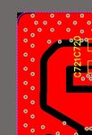
I designed a 8W GSM module, and the attached JPG is the 8W GSM TX trace.
The trace width is 2.7mm, and the around vias are ground.
The clearance between the GND and the trace is 1mm.
I doubt is it enough of the 1mm clearance?
If the 1mm is too narrow, would it cause any spurs in 500M-800MHz?
Best,
Tony Liu

- - - Updated - - -

PS: the DC is 12V.
 

Attachments

  • C1.JPG
    C1.JPG
    26.3 KB · Views: 124

How should transmission line geometry related to spurs? I presume you'll want to implement 50 ohms impedance. Dielectric strength required for 8W isn't so critical.

There seem to be misplaced ground vias.
 
the top ground pour being 1 mm away causes excess capacitance. Consequently, you have to narrow the trace width to maintain 50 ohms. Did you calculate the trace width with that in mind, or did you ignore the capacitive effect???
 
Hi,
I used the LDMOS, i.e. AFT09MS015N, and copied its recommended 870M circuits. So the impedance should be OK.
Now the PA worked fine.
Only with a spur -38dBm@700MHz, but standard is -36dBm.
So it can pass TA.

I only doubt if the spur is caused by PA itself?

Best,
Tony Liu
 

Attachments

  • AFT09MS015N-783349.pdf
    854.4 KB · Views: 111

I'm wioth FMV & bif44 on this. I doubt the spur is being caused directly by the gap-to-ground but notice that there is vias in that gap. That gap-to-ground has to be doing odd things to your impedance. While waiting for a simulation to finish, I ran TXLine... I don't see this tracewidth and gap calculating to be 50ohms. The two tight bends so close together could also do strange things to impedance, but that could be a design trade-off.
 
Non-harmonic spurs are a PLL problem and can't be generated by the PA.
 
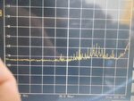
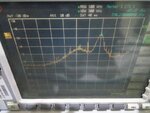
Here is the comparison of the Mitsubishi PA and NXP PA.
The main signal is at 887M GSM with 39dBm, the insertion loss is 8dB for freq <=885M.
Mitsubishi PA causes some spurs at 770M, but the spurs level are below -55dBm.
NXP PA causes spurs at the same freq, but the levels are about -47dBm.
Both with the same input.
The standard are below -36dBm, if added 8dB, i.e. -44dBm.
So I think that is the difference of the PAs, different PA cause different spur level.
 

Attachments

  • Mitsubishi_PA.jpg
    Mitsubishi_PA.jpg
    48 KB · Views: 115
  • NXP_PA.jpg
    NXP_PA.jpg
    50.1 KB · Views: 119

Spurs can be sourced by different reasons such as power supply originated,grounding and layout originated,circuit itself,decoupling,external unwanted coupling,nonlinearity,measurement equipments etc.
It's really difficult to say something consistent without examining the circuit.
 
Status
Not open for further replies.

Part and Inventory Search

Welcome to EDABoard.com

Sponsor

Back
Top