Continue to Site

Welcome to EDAboard.com

Welcome to our site! EDAboard.com is an international Electronics Discussion Forum focused on EDA software, circuits, schematics, books, theory, papers, asic, pld, 8051, DSP, Network, RF, Analog Design, PCB, Service Manuals... and a whole lot more! To participate you need to register. Registration is free. Click here to register now.

[SOLVED] Strange EM cosimulation, Keysight ADS

Status
Not open for further replies.

circuit_hunter

Junior Member level 3
Joined
Jan 8, 2017
Messages
25
Helped
1
Reputation
2
Reaction score
1
Trophy points
3
Activity points
344
Hi

I am doing emcosimulation of an Rf rectifier.
Please consider the following figure:
Fig1.PNG

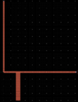
Part B contains the pads for diode and lumped components (boxed) plus an additional line. I EM cosimulated this , found the input impedance, and designed a matching network shown in Part A (boxed). I connect them (point 1 to point 2), and EM cosimulate it, gives decent performance with 60% peak efficiency. Please note that PART A is much bigger as compared to PART B, I have scaled its sybmol for clarity.

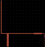
Now I make complete layout, drawing PART A and B in the same window as shown in the following figure:
Fig2.PNG

I EM cosimulate this and efficiency is 3% !

The diode and lumped element and dimensions of each lines, everything are the same but still this poor performance is strange. Any idea why it would happen?

Thank you in advance for your precious time.
 

Attachments

  • Fig1.PNG
    Fig1.PNG
    12.4 KB · Views: 306

What are the dimensions of your structures and frequency range? How do you calculated and designed the matching network?
 

The matching circuit seems to be unusual.I guess there are some mistakes..
 

Thanks for the quick response.

The dimensions of PART A is 2200mil*1400mils and that of the PART B is 800mils*300mils. The design frequency is 900MHz. I used HB/LSSP to find the input impedance of PART B and invoke my analytically derived equations to design the matching network. I observe the following cases:

(1) I design the matching network (PART A) using ideal lines and append it to the em model of part B- It works as expected.
(2) I design the matching network in microstrip and append it to the em model of part B- It works as expected.
(3) I design the matching network in momentum and append its em model to the em model of part B- It works as expected.
(4) I put the combined structure in momentum and generate em model, simulate it in em cosim- It DOESN'T work.
(5) Even if i tried to put PART A and B far apart in momentum, defining points 1 and 2 as ports (with TML zero length calibration) , generate em model and join points 1 and 2 during EM cosim- It DOESN'T work.

@Bigboss: Sir why the matching network looks unusual? Its just a T-network. And since it works in above cases 1 to 3, there doesn't seem to be problem with the matching. But, I will definitely check this, again.

I wonder if it could be port settings creating the problem? In PART B, I define ports as default TML ports. I have tried area pins also, but the results are almost the same.

- - - Updated - - -

The reason I suspect the port settings might be creating the issue is the following warning message that I get while simulating PART B alone or together (with PART A):

Fig3.PNG
 

Check the input impedance for case (3) and (4) at the input of the matching network, are they the same? Why you use tml-matching circuits at 900 MHz? Maybe it's space-saving to use discrete components instead. Where are ports 10 & 11? Are the simulation settings (mesh density etc.?) equal for cases (3) and (4)?
 

Also check defined port impedance for EM simulation, is it same for all port?
 

@BigBoss: I checked the matching network by terminating it with the impedance of PART B, which I had obtained using LSSP/HB simulation, and it works fine. But, you might have a point: The input impedance was calculated with power injected at the input of PART B. But, when I include the matching network, the same amount of power will not reach to part B and hence the impedance will be different for SBD impedance is power dependent. However, if this were really the case, then why would it work in case 2 and 3?

@John: Of course the input impedances are different that's why the results differ. Port 10 and 11 etc are ports inside the PART B for SMD elements and diode connections. I have kept the mesh density and every other parameter the same. I am just testing it at 900MHz, later I will increase the frequency- that's why I am not using lumped element for matching. I found it very difficult to find inductor and capacitors beyond 2GHz and with good quality factor. If you know any good series for L and C with good quality factor at around 3GHz, please let me know, I will make another version with lumped elements.

@ Anil: I keep all the port impedances to the default value of 50 ohm.

I always do EM simulation the way I am doing. I have seen people successfully designing matching networks for PA independently just based on load impedance obtained from load pull simulation and this case is similar to mine except I obtained impedance from LSSP/HB , but I don't know why this abnormal behavior is happening with rectifier. I have tried in different ways for last ten days, but its not working. It work very good in schematic with microstrip lines and when simulating with em models of individual blocks. I forgot to mention, the substrate is Rogers with Er=3.55, tanD= 0.002, 20mil height , 17.5um copper both sides.
 

What kind of port are you using at Part B input?
 

Thank you so much for your time, John. All the ports in Part B are TML , except the input (point 2) which is TML (zero length). But, I think internal ports are also changed to TML zero length as line extension required in TML will intersect other lines. In anycase, port calibration shouldn't make that much difference, I guess.

However, I did more simulations, and now I think I know why this anomaly is happening, let me tell you about the my matching network (PART A) simulation which I initially thought was not important:

I designed the matching network using analytical equations for the load obtained earlier from PART B LSSP/HB, implement it in microstrip, optimize it there and then I perform its momentum simulation to create an EM model. But, during momentum simulation it gave me a warning:

"Automatically determined a snap distance of
0.0021 mil for layout healing.
--- WARNING -------------------------------------------------------------------
Layout healing changed the layout. The actual
highest aggregate snap distance was 0.0001 mil.
Further details have been written to the DRC
report."

I ignored this warning inspired by Dr Volker's comments: **broken link removed**

Then, I optimize the EM model of the matching network in EM cosimulation for the load obtained earlier from PART B.

Rest of the story you know, I simulated EMmodel of the (optimized) matching network and that of the PART B, it works; and when I draw combined layout then it doesn't.

Now, I suspect its ignoring layout healing that might be causing the problem. My reason is as follows:

(please see case 5 in above message in this thread) I put PART A and B far apart in momentum, defining points 1 and 2 as ports (with TML zero length calibration) , generate em model with layout healing enabled as has been the case so far:

(1) I find input impedance looking into PART B from point 2, its way too different than the initially obtained from EMsimulation of PADS.
(2) Then I turnoff layout healing and generate EMmodel and this time the input impedance is the same as previously found from simulation of PADS. But, If if look input impedance from point 1 of PART A ( terminating its input to 50 ohm), it is NOT complex conjugate!
(3) I again turn on layout healing, find the input impedance from point 1 of PART A ( terminating its input to 50 ohm), it is complex conjugate of original load!

From these observation, I conclude that PART A likes layout healing whereas PART B doesn't when I draw the combined layout.

So what do you guys suggest me the next thing to do? And if the momentum is changing my layout, isn't it a bad thing?
 

I don't think that "layout healing" changed your layout significantly, just have a look at the snap distance for layout healing and compare the value to your structure. They differ in magnitude. Can you upload your design folder here?

- - - Updated - - -

In addition, i tried to verify your problem with two separate structures and both combined: Both results are quite equal.

- - - Updated - - -

Attached the results:
struct_a.PNGstruct_b.PNGstruct_combine.PNG

results.PNG
 

Thanks for your efforts, I appreciate the simulations results. I have sent you the files privately.
 

I have an idea what is your actual problem:

What I have done:
1) I used both structures in a schematic, single structure A and B, connected via an wire, and A and B combined via EM-sim. I simulated small signal s-parameter without lumped components -> almost identical
2) I added passive components, small sig s-parameter -> almost identical
3) Added your diode with model, small sig s-parameter -> almost identical
4) Switched to large-signal s-parameter -> different results
5) Replaced diode with resistor, large signal s-parameter -> almost identical

The problem is the frequency range of your EM-simulation. You start at 0.5GHz, and frequencies below (especially at DC) are linearly extrapolated, and these results differ!
So in the case of LSSP, the operating points of your diode differ and you get different results!

Extend the frequency range of your EM-simulations down to 0 Hz.

- - - Updated - - -

Your pad and matching structures (separated or combined) works fine. The problem is the active component.
 
I was about to give up on this as many of my design used to fail coming at last stage. So, thanks a so much, John. Thank you for your precious time.

I have couple of more questions:

(1) Do you suggest whenever I use active device, I should do momentum from 0 Hz?

(2) Why do I get warning about port not being on edge of conductive/nonconductive layer (please see 4th message above)? Can I ignore this warning?

(3) I read couple of documents on area/edge pin types, especially:https://literature.cdn.keysight.com/litweb/pdf/5992-0415EN.pdf, and I guess wrong usage may cause small error compared to measured result. Should I use edge/area pin or the default one as I have been doing so far?

(4) Is there anything else I need to care about or I am good to go for prototype fabrication if I consider my results satisfactory?
 

I was about to give up on this as many of my design used to fail coming at last stage. So, thanks a so much, John. Thank you for your precious time.

You're welcome!

(1) Do you suggest whenever I use active device, I should do momentum from 0 Hz?
You have to because the DC current path is extracted from higher frequency. In your case above, the DC characteristic of your structure is calculated from the characteristic at 500 MHz, and this is for sure not correct.

(2) Why do I get warning about port not being on edge of conductive/nonconductive layer (please see 4th message above)? Can I ignore this warning?
You placed some of your ports in structure B inside the structure:
1.PNG
ADS can't extend the transmission line for calibration, and chose "None" as calibration type. In the case of smd components it should be ok to do so. Maybe take a closer look at calibration type "SMD" in the online help. To deactivate the warning set calibration type to "None".

(3) I read couple of documents on area/edge pin types, especially:https://literature.cdn.keysight.com/litweb/pdf/5992-0415EN.pdf, and I guess wrong usage may cause small error compared to measured result. Should I use edge/area pin or the default one as I have been doing so far?
It depends on your application, will you place components or is this your RF feed. I think all options are well explained in 5992-0415EN, and thanks for the link!

(4) Is there anything else I need to care about or I am good to go for prototype fabrication if I consider my results satisfactory?
How much experience you have? In my personal opinion, there will be always a mismatch between simulation and measurement.
 

Thanks, again. And sorry for delayed reply I got busy in some write up.
It depends on your application, will you place components or is this your RF feed. I think all options are well explained in 5992-0415EN, and thanks for the link!

This an academic project, so may be this will be standalone circuit. Or may be, later, I can use it with antenna and some storage element.
But, in any case I will more port calibration type and compare that with the measurement results.

How much experience you have? In my personal opinion, there will be always a mismatch between simulation and measurement.

I did only passive so far. Last time I tried to design an RPFA, it had similar problems, now I know where the problem was coming from- I was missing DC. Hopefully I will try to restart that design. But, I do agree that even in passive when I used lumped elements, the simulation and measurement do differ much.

Lastly, thanks a lot for your time, I learned a lot here. Marking this solved.
 

Status
Not open for further replies.

Similar threads

Part and Inventory Search

Welcome to EDABoard.com

Sponsor

Back
Top