Continue to Site

Welcome to EDAboard.com

Welcome to our site! EDAboard.com is an international Electronics Discussion Forum focused on EDA software, circuits, schematics, books, theory, papers, asic, pld, 8051, DSP, Network, RF, Analog Design, PCB, Service Manuals... and a whole lot more! To participate you need to register. Registration is free. Click here to register now.

EMC designing questions for PCB

Status
Not open for further replies.

Ranbeer Singh

Full Member level 5
Full Member level 5
Joined
Jul 30, 2015
Messages
259
Helped
22
Reputation
44
Reaction score
22
Trophy points
1,298
Location
Faridabad India
Activity points
3,266
Hello friends,

I have solved many of my critical problems with help of yours and i am so obliged for your helps.

At this time my concerned was for designing a bus door's controller PCB with electromagnetic compatibility (EMC). Honestly i don’t have a good knowledge of EMC designing for PCB.

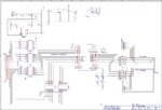
Controller circuit is given in attachment, i am using through-hole components & there is no analogical circuit inside. I read in a book that we would be most carefully design with through-hole components. I know... respect to switching output signals, basically, only worry about signals that make an edge transition at a rate greater than 50 kHz. If a pin changes its state at a rate of less than once per 100 instructions, this is acceptable because the contribution from switching is negligible. If the pin toggles, and toggles back on the next instruction, and remains static for 100 instructions, it, too, is acceptable because it contains the same amount of energy.

My all inputs & outputs will not work on high frequencies. It will work less then 1Hz but may be
there will be other types disturbances like EMF, ESD, EOS & etc.

Someone said me that EMC testing procedure is very costly. So i am afraid and not able to pay off it's cost 2-3 times.

Please help.
 

I don't see the attachment and to be honest I don't know what a bus door controller is ;-)
I can however give You a few hints on proper design procedures for EMC.
Most important is a decent low impedance ground structure.
For radiated fields provide a path where these disturbances can flow without upsetting your micro,
place a (small) capacitor with a low impedance in the frequency range of interest close to the inputs.

With your transitions it is not about how oft You switch, it is more about how fast your transition go from low to high.
I experienced a 19 kBaud data transmission with a 1,5 meter cable with a transition speed of 0,8 ns.
The communication was slow but it was very clear measurable in the radiated emission.

ESD, You have to protect the lines which can be accessed.
I oft use 500 mW zeners for this purpose, this will clamp the voltage to safe levels.
(as long as the ESD isn't injected more or less constant)

I don't know for which market this is or to which standards You have to comply.
With a bit more info I might have some other hints.
 
I am sorry for forget to attached the file. Please check the attached file. file-page1.jpg


All circuit (input, output & power) will use 24VDC. I was thinking to change input circuit with as voltage divider. Will it be correct or not?

- - - Updated - - -

We are building this controlling system for VOLVO, TATA..... bus door controlling.
In India, though there is no regulation on EMC compliance, STQC (standardisation, testing and quality certification) directorate formulated a “EMC Compliance Certification Scheme” to enable Indian manufacturers to meet various IS, EN, FCC, IEC EMC standards requirements
 

Hi,

* solid GND plane
* a fast ceramics capacitor at each IC's supply pin.
* aviod ESD currents to cross the GND plane under the microcontroller
* HF filtering on each line leaving the PCB
* overvoltage protection on each line leaving the PCB
* a LPF on each sensitive line on the PCB ( reset line for example)

Klaus
 
I won't expect active EMC (emission) problems for a single processor with internal oscillator, although you'll probably want more than one tiny 100 nF supply bypass capacitor.

Passive EMC (susceptibility to RF interferences and ESD immunity) will be most likely a problem as the design lacks any suppression means.

It's also obvious that the circuit isn't designed in aware of standards like ISO16750 and ISO7637. It will probably fail most relevant tests.

Try to understand the requirements. You don't necessarily need to perform costly tests in an approved lab, start to consider the standards and make some basic pre-compliance measurements.

By the way, it's always confusing to read a schematic with implicit (hidden) supply connections.
 
I have to say I agree with FVM,
immunity might be a problem when I see this schema.
First read to what standards You have to comply, and which test levels You have to fulfill.
With this in mind You start your designing and your layout.
 

Have a look at the UK EMC club, if you sign up for the site you can get to some good info from Keith Armstrong. Also look at Henry Ott and Ralph Morrison's sites.
 

Thanks to all

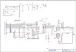
I modified my circuit as per #4 & #5. Please check it.


file-page1.jpgL01_TOP-1.jpgL02_BOT-1.jpg


I want to measure ESD, EOS, EMF & surge only. All circuit will work less then 1Hz and using internal 4Mhz oscillator for microcontroller.

My concerned ware :
1. I changed digital input circuit with divider instead to opto base of my last thread "24VDC to 5VDC level converter ic". In this thread ClausST says
In general resistors are relatively robust against overvoltge and they limit current and divide voltage.. additionally they transform the electrical energy into heat.
2. Will need of copper ground pour in case of 1Hz circuit?
3. Any mistake in my circuit?
4. I am using ULN2003A for output. It have internally suppression diodes are included for inductive load driving. External suppression diode will be need?
 

Hi,

Did you follow a single point of my recommendations of post#4?

* no GND plane, even a copper pour is far away from being a solid GND plane.
* capacitors are missing, pin32 of PIC isn't connected at all (it's not by accident called VCC)
* you did feed the complete output GND (including ESD) current explicitely under the PIC with a thin wire
* HF filters are only on the signal input lines
* overvoltage filters are missing completely
* LPF filters on sensitive lines are missing completely

Sorry, i have to say it's far away from being a reliable design

******
What's the purpose of Q1?
You have a lot of current at the outputs. Did you follow it's path (it doesn't stop at the ULNs). Did you calculate trace width?
A 1000uF input capacitor will cause a lot of input current when connected to 24V.
GND pins are missing at the input connector and the output connector.
Did you calculate the power dissipation of the output pullup resistors?

I'm stoping here to check your circuit....

Klaus
 
Will need of copper ground pour in case of 1Hz circuit?
Not for a 1Hz circuit as such. But you need stronger ground connections to handle the output currents claimed in the schematic. And you surely need it if you start to add serious ESD and surge protection.

The 0.5/1.0/1.5 A output current specifications are not substantiated by ULN2003 datasheet, by the way. 0.5 A is only valid for one activated output, review the allowable collector current graph.

State-of-the-art suggests short circuit and overcurrent protected smart power switches instead of ULN2xxxx.
 
Did you follow a single point of my recommendations of post#4?

* no GND plane, even a copper pour is far away from being a solid GND plane.
* capacitors are missing, pin32 of PIC isn't connected at all (it's not by accident called VCC)
* you did feed the complete output GND (including ESD) current explicitely under the PIC with a thin wire
* HF filters are only on the signal input lines
* overvoltage filters are missing completely
* LPF filters on sensitive lines are missing completely

Sorry, i have to say it's far away from being a reliable design

******
What's the purpose of Q1?
You have a lot of current at the outputs. Did you follow it's path (it doesn't stop at the ULNs). Did you calculate trace width?
A 1000uF input capacitor will cause a lot of input current when connected to 24V.
GND pins are missing at the input connector and the output connector.
Did you calculate the power dissipation of the output pullup resistors?

Thenk you very much

These point are like treasure for me. Yes i except that i did not implement those point to well.

* I read a book on ground plan and your instructions. I may be now will improve/correct.
* what capacitors am i missing? Pin32 of controller is VCC and my software connect all same name net pins to each other automatically.
* I was waiting to clear my circuit first.
* where will need of HF filters except to inputs?
* I wanted to make my PCB small as possible. So I skipped knowingly those circuits.

****
* I used Q1 for power input polarization inversion protection.
* I will do these after complete my circuit. If i change in my circuit, these work will be worthless.
* what will be wrong with 1000uf capacitor?
* Ground pins with input output connectors is nice prectice. I will implement it.
* I do not know pullup resistence calculation according to ULN. Please explain.


Not for a 1Hz circuit as such. But you need stronger ground connections to handle the output currents claimed in the schematic. And you surely need it if you start to add serious ESD and surge protection.

The 0.5/1.0/1.5 A output current specifications are not substantiated by ULN2003 datasheet, by the way. 0.5 A is only valid for one activated output, review the allowable collector current graph.

State-of-the-art suggests short circuit and overcurrent protected smart power switches instead of ULN2xxxx.

Thank you for your replies

Although my all output are less then 0.2A. However the ST ULN2003A datasheet says that "Outpu can be paralleled for higher current outputs". Is it not correct?
 

Hi,

* what capacitors am i missing? Pin32 of controller is VCC and my software connect all same name net pins to each other automatically.
--> the capacitor at pin 32 is missing
now I see there is a VCC connection in the PCB. But the is not obvious in your schematic. Maybe you know that it is connected, but we don´t.
It is more obvious if you connect them in schematic.
A benefit is, that you recognize the missing capacitor.

******
GND plane:
With the high GND currents, i assume a 2 layer PCB will not do. Not with the GND path now.

*****
* where will need of HF filters except to inputs?
post#4: * HF filtering on each line leaving the PCB
Input as well as outputs and power. At least for a good EMV design, where cable induced high voltage/ high frequency signals may affect your circuit.

*****
* I wanted to make my PCB small as possible. So I skipped knowingly those circuits.
If yo want it small, then use SMD. This additionally increases the chance for a two layer PCB, becuase the pin´s don´t split the GND plane at the bottom side. But it´s no guarantee.

*****
* I used Q1 for power input polarization inversion protection.
I don´t like switches in the GND line of a power supply. If the switch is open, then you loose GND as reference. This may cause that the resistive dividers at the 24V signal input don´t work anymore.
--> Check signal integrity when Q1 is open.

*****
* what will be wrong with 1000uf capacitor?
Calculate the inruh current. I assume it easiyl can be well above 50 Ampres. Is your design made for this?
If so, then at least I told you to take care...

*****
* Ground pins with input output connectors is nice prectice. I will implement it.
No. It´s not nice. IT IS URGENT! Otherwise all the load current is flowing across the complete PCB.

*****
* I do not know pullup resistence calculation according to ULN. Please explain.
Did you calculate dissipated power? Can your resistors withstand it?
I dont know the specifications of your resistors. Only you know....


Klaus
 
I used Q1 for power input polarization inversion protection.
Unfortunately the circuit doesn't work. The MOSFET should be turned on with correct polarity and turned off for inverted input voltage, but it isn't. Use a PMOS switch in positive supply line or a NMOS switch in negative supply line to achieve the intended effect.

However the ST ULN2003A datasheet says that "Output can be paralleled for higher current outputs". Is it not correct?
That's correct, but you need to consider the derating given in the datasheet. The current values written in your schematic can't be achieved.
 

post#4: * HF filtering on each line leaving the PCB
Input as well as outputs and power. At least for a good EMV design, where cable induced high voltage/ high frequency signals may affect your circuit.

But in my circuit no more current & no high frequency.

I don´t like switches in the GND line of a power supply. If the switch is open, then you loose GND as reference. This may cause that the resistive dividers at the 24V signal input don´t work anymore.
--> Check signal integrity when Q1 is open.

Yes you are right. I tested it and found if Q1 is open/damaged, digital input voltage goes to MCU pin is 24v. I want to change it circuit with a diode or relay circuit. What will be best?
 

Hi,

But in my circuit no more current & no high frequency.
I agree. Your signals.

But the ESD and EMI signals are HF. And you have to take care about them.

Imagine a relay switching next to your application, an RF source (cellular phone..) next to your PCB...

Klaus
 

Status
Not open for further replies.

Part and Inventory Search

Welcome to EDABoard.com

Sponsor

Back
Top