xuyue1983
Newbie

- Joined
- Feb 7, 2012
- Messages
- 3
- Helped
- 0
- Reputation
- 0
- Reaction score
- 0
- Trophy points
- 1,281
- Activity points
- 1,328
Hi all,
I have a very straightforward requirement:
I need to test my own chip (ASIC).
1st step: Load data from my computer to a RAM. The data width is at most 32 bits. This process does not need to be very fast.
2nd step: Read the data sequentially from the memory and give the data to my chip, which takes in 32bits in parallel. The data rate has to be at least 100MSPS. And I want to be able to control the data rate (by programming the FPGA?)
I would like to know if this is achievable using VC707 evaluation board or other lower end FPGA evaluation board.
I browsed through VC707's user guide and schematic. VC707 Evaluation Board has a DDR3 (Module density: 1GB, 128 MegX64, Module Bandwidth 12.8GB/s, Memory Clock/Data Rate 1.25ns/1600 MT/s) and FMC HPC1/HPC2 Connectors.
Could you please give me some guidelines on how to do this? I have some vague ideas that I may need a memory controller. But it's not very clear if that is the correct path to go.
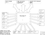
This is VC707 Evaluation Board's diagram:

The schematic of VC707 can be downloaded from https://secure.xilinx.com/webreg/cl...c707_Schematic_xtp135_rev1_0.pdf&languageID=1
The user guide of VC707 can be downloaded from https://www.xilinx.com/support/documentation/boards_and_kits/vc707/ug885_VC707_Eval_Bd.pdf
Thank you very much!
I have a very straightforward requirement:
I need to test my own chip (ASIC).
1st step: Load data from my computer to a RAM. The data width is at most 32 bits. This process does not need to be very fast.
2nd step: Read the data sequentially from the memory and give the data to my chip, which takes in 32bits in parallel. The data rate has to be at least 100MSPS. And I want to be able to control the data rate (by programming the FPGA?)
I would like to know if this is achievable using VC707 evaluation board or other lower end FPGA evaluation board.
I browsed through VC707's user guide and schematic. VC707 Evaluation Board has a DDR3 (Module density: 1GB, 128 MegX64, Module Bandwidth 12.8GB/s, Memory Clock/Data Rate 1.25ns/1600 MT/s) and FMC HPC1/HPC2 Connectors.
Could you please give me some guidelines on how to do this? I have some vague ideas that I may need a memory controller. But it's not very clear if that is the correct path to go.
This is VC707 Evaluation Board's diagram:

The schematic of VC707 can be downloaded from https://secure.xilinx.com/webreg/cl...c707_Schematic_xtp135_rev1_0.pdf&languageID=1
The user guide of VC707 can be downloaded from https://www.xilinx.com/support/documentation/boards_and_kits/vc707/ug885_VC707_Eval_Bd.pdf
Thank you very much!

