Continue to Site

Welcome to EDAboard.com

Welcome to our site! EDAboard.com is an international Electronics Discussion Forum focused on EDA software, circuits, schematics, books, theory, papers, asic, pld, 8051, DSP, Network, RF, Analog Design, PCB, Service Manuals... and a whole lot more! To participate you need to register. Registration is free. Click here to register now.

TIG Welder, inverter gate driver

Status
Not open for further replies.

masterx81

Member level 1
Member level 1
Joined
Apr 5, 2002
Messages
40
Helped
6
Reputation
12
Reaction score
6
Trophy points
1,288
Activity points
339
Hi!
I've "repaired" a chinese TIG welder (repair is a big word, only had cold solders, loose fastons, loose screws that must handle 200a, etc. Nothing burnt) and i'm studying the circuits for try to improve them.
I have a basic understanding of swtiching technologies (i know how they work and with some limits i can repair them), but i not know every aspect. I've learned on the net how a mosfet must be driven, the Qg curve, conduction and switching power loses, etc, but would be great to have some advice... I use this welder as a "learning bench" as have quite simple circuits (i've followed the tracks and i have all the schematics of the whole circuits :bang::shock::-D), and as far i can understand, it's not much optimized.
I've started to analyze the inverter, it have an H bridge composed of 3 paralleled n-channel mofets (23N50E - **broken link removed**, every of them have a 68ohm gate resistor) per branch, the output of the H bridge goes to 3 power transformers (via 3 4,7uF capacitors).
The chip controlling the the bridge (via an isolation transformer) is a KA3525A, the calculated switching frequency is 115khz (c=1nF, R=6.2k).
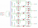
This is the schematic of the driver:
Gate driver
gate.PNG
And this is the output (at the gate, after the 68 ohm gate, DC trace source-gate):
Low side
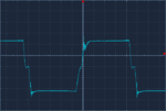
Low1-Post-R.PNG
High side
High1-Post-R.PNG
1uS/div, 5v/div for both, near 30vpp, the actual switching frequency is 103.1khz

This is how the isolation transformer is driven (24v supply, with h bridge at the output of the 3525):
Transformer input
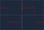
Pilotaggio.PNG
1uS/div, 10v/div, 50vpp

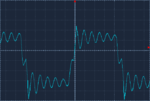
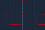
The first thing that i notice is that bad oscillation on the high side (why is present on the high side but not on the low side? Error itroduced by oscilloscope?), second one is the little ringing also on the low side, third one is that the gate is driven at much less the 10v reccomended for complete gate closing,
I've still not calculated the correct gate charge/switching power losess (first i've had the need to measure what was the voltage swing on the gate)
So, to my limited understanding, i would say that is better to create a new gate driver that reach at least the 10v gate charge, eliminate that oscillation on high side and check the switching losess to see if there is enough gate charge...
Can someone please help me, and tell me if i'm going in the wrong direction?
Really thanks, any help is much appreciated :-D
 

Could you post the whole schematic that you traced out.
 
  • Like
Reactions: jardo

    jardo

    Points: 2
    Helpful Answer Positive Rating
I've traced ALL, also logic board (as i'm intended to replace the whole board with an improved ucontrolled version - i do program uC).
What part are you interested?
 
I would like to see all of it.
 

I'm in the process of transfer the schematics from paper to kicad (on paper are not too much readable), for now i have completed the power supply board/HV board, diode board, ACDC gate driver board and some parts of the inverter board, if you have patience to wait a bit i complete the job, or you prefer a scan of the paper?
No much surprise on this schematics, the signals are generated via opamp and logic ports, and an analog switch for selecting the various current settings based on timings. The AC/DC inversion in done with an H bridge of 8x fets paralleled per branch (and also here the gate driver is really minimal, switching losess are not much important as ac/dc switching frequency is only 60hz), the hf shuts down based on output voltage...
The diode board has a shunt resistor for current sensing, and the inverter board/ka3525a choose the duty based on this feedback versus the voltage set by the pots.
Some circuits are so simple that i'm suprised how they works well.
On the net i've found this schematic:
View attachment TIG200PACDC iagram.pdf
That is quite close to my welder, but miss some board details (like the inverter driver circuits) and differs on some minor things.
 
It looks like the pdf has a bridge driver chip directly to the gates and yours has a gate transformer.

I am very interested in welders from the high power design point and the high frequency/arc starter circuits. I will wait for your CAD schematic and i hope you post some pictures of the electronics especially the power and starter sections.
 

Hi!

So, to my limited understanding, i would say that is better to create a new gate driver that reach at least the 10v gate charge, eliminate that oscillation on high side and check the switching losess to see if there is enough gate charge...
Can someone please help me, and tell me if i'm going in the wrong direction?
Really thanks, any help is much appreciated :-D

The ringing on the high side gate doesn't look real. Try to disconnect the high voltage to the drains of the high side, and look at the gates drive again. If the ringing goes away then it could be something to do with the oscilloscope.
 
I think that is an error of the measurement too as there isn't any resonance near vgs (miller zone). I not know how was inserted... I've isolated the groud of the scope (paying attention to not touch metallic things, as i haven't an isolation transformer under the hands), maybe this is the cause.

- - - Updated - - -

It looks like the pdf has a bridge driver chip directly to the gates and yours has a gate transformer.

I am very interested in welders from the high power design point and the high frequency/arc starter circuits. I will wait for your CAD schematic and i hope you post some pictures of the electronics especially the power and starter sections.
Will do it :D

- - - Updated - - -

Strange thing is how dc is passed through the transformer...
 

switching losess are not much important as ac/dc switching frequency is only 60hz
Where? The TIG inverter is using high kHz frequency.

I've isolated the groud of the scope (paying attention to not touch metallic things, as i haven't an isolation transformer under the hands), maybe this is the cause.
Apart from being quite dangerous, the method can't be expected to give acceptable measurement signal quality. Isolation transformer isn't much better for measurements at fast switching circuits with superimposed high frequent common mode signals, HV differential probe is the only reasonable option.
 

Where? The TIG inverter is using high kHz frequency.
TIG uses HF to generate isolated high current DC (basically switcher instead of the traditional heavy transformer). After that the DC is converted to 60Hz by another inverter which drives the electrodes.
 
  • Like
Reactions: FvM

    FvM

    Points: 2
    Helpful Answer Positive Rating
Yes, as in the previously attached circuit, thanks.

For some reason, I was thinking of a DC welder and didn't notice the inverter.
 

Apart from being quite dangerous, the method can't be expected to give acceptable measurement signal quality. Isolation transformer isn't much better for measurements at fast switching circuits with superimposed high frequent common mode signals, HV differential probe is the only reasonable option.
Hum, seem a thing to be added to my tools... They seem quite expensive (half the costs of the scope 8-O:lol::lol: ).
It's the first time that i do this type of measurement so i've used what i've had under the hands and not knew what was better. I will try to find one, thanks for the suggestion :thumbsup:
So the high side trace is useless, but the low side one seem quite realistic...

- - - Updated - - -

Uhm, maybe i can try to use the math function of my dual channel scope? I get best results? I was searching but that probes costs really a lot :cry:
And as i will use it only in really few occasions, i'm not sure if it worth...
I've also seen some DIY projects over the net, but i'm unsure about the quality...

Maybe you should give more serious consideration to my advice in post #7.
 

Maybe you should give more serious consideration to my advice in post #7.
Done:
High side isolated.PNG
This is with inverter powered but 300v disconnected from the high side fets.
Please, correct me if i'm wrong, I think that they have put the zener on the driver circuit (on pos #1) for have a negative bias on the output of the isolation transformer, because the deadtime of the 3525 (set to it's minimum with a 1nf capacitor ad Rd=0ohm) was slowing down the closing and opening of the gates. But why 5v, while was sufficient a lot less (for have more voltage on the gate and lowering the Rdson?
And why the DC is passed on the output of the transformer? I wan't expecting an output waveform like this...

Thanks for the suggestions...

- - - Updated - - -

And as promised some schemes.
This is the diode board (after the inverter).
diode.PNG
It has 3 paralleled transformers (1 primary and 4 secondary), any of them have it's input connected to the output of the inverter via a 4,7uF capacitor.
Only one of them have the thermic protection (that goes to the inverter for shutdown of operation).

This is the driver of the board that invert the signal and generate the AC waveform:
ACDC.PNG
4 identical stages, each of them drives 8 paralleled irfp260m, with an 51ohm gate resistor for each one.

This is the HV section:
hv.PNG
X3 goes to the output of the AC inverting board
X4 to the switched exit of the inverter (via a 4.7uF capatitor)
CP1 and CP2 goes to the output trasformer for inject the high voltage

And this is the power supply, protection circuits and gas valve circuits.
power suplly.PNG

- - - Updated - - -

One more question, why they have used the 3525 in pushpull mode? what advantage there is driving ah isolation transformer?

Sorry for the numerous questions, but i'm curious to understand why they have taken some design decisions...
 

Leave the supply to the drains disconnected, reverse one or all of the zeners and check if you like the gate drive better.
If you have a variable power supply connect it in place of the supply to the drains of the high side and check if the inverter output looks better with the zeners reversed.
Maybe these tests will help you get into the mind of a Chinese engineer.
 
Uhm, but inverting the zener will not have the effect of negative biasing the signal of only 0.6v? This will be good as i can have 4.4v more on the gate for complete closing without have the deadtimes introduced by the pushpull operation of the 3525, but i really not understand the purpose of putting a so high negative bias... Maybe with load the waveform can change and the chinese engineer wanted to be sure of the complete opening of the fet?
A side effect of inverting the zener is that retains the function of providing a path for the discharge of the gate (until there is a difference of 5v, but when there is less than 5v the gate is already opened as the surce-gate voltage is already negative).
I'm also simulating the circuit with ltspice and inverting the zener seem to increase a bit the current flowing on it, but still in a allowable range. (yes, i've read you signature and i was laughing while writing :D :D)
There is a correction on the scheme on the post #1, the gates of the fets have a 6.8ohm resistor, and also the driver resistor is a 6.8ohm (not 68ohm).

Need really to do some math and calculate power losess and correct gate charge... Now i have all what is needed :p
 

The simulator in my brain tells that if you reverse the zener the gate drive will swing from +12V to -5V.
I know little about simulators. Can your simulator give a picture of the gate drive? can you post the picture in a picture type file (gif, jpg, etc) ?
 

The simulator in my brain tells that if you reverse the zener the gate drive will swing from +12V to -5V.
I know little about simulators. Can your simulator give a picture of the gate drive? can you post the picture in a picture type file (gif, jpg, etc) ?

Uh, i've already shut off the pc (i'm going to bed, but tomorrow i can put a screenshot), but for have a total inversion of the bias i've had to invert also the diode in series at the 3k resistor.
Only inverting the zener gave me a 0.6v negative offset instead of 5v.
 

This is the simulation plot:
Immagine.PNG
Blue trace out of the transformer, green trace at the exit
Top simulation is with zener placed as engineers put it (5v negaive bias, as measured), bottom one is with zener inverted (0.6v negative bias)
 

It looks like my simulator agrees with yours.
Is the gate drive good for you?
 

Status
Not open for further replies.

Similar threads

Part and Inventory Search

Welcome to EDABoard.com

Sponsor

Back
Top