Continue to Site

Welcome to EDAboard.com

Welcome to our site! EDAboard.com is an international Electronics Discussion Forum focused on EDA software, circuits, schematics, books, theory, papers, asic, pld, 8051, DSP, Network, RF, Analog Design, PCB, Service Manuals... and a whole lot more! To participate you need to register. Registration is free. Click here to register now.

multi voltage power supply

Status
Not open for further replies.

aliyesami

Full Member level 6
Full Member level 6
Joined
Jan 7, 2010
Messages
369
Helped
0
Reputation
0
Reaction score
0
Trophy points
1,296
Location
USA
Activity points
4,190
I want to build a 3.3v, 5v DC power supply which will be fed off by an AC-DC adaptor.
I need 2Amp for 5V , 500mA for the 3.3V .
is there any one chip that can do that ?
i want to keep the supply compact.

thanks

- - - Updated - - -

btw iam going to use a 12v 5amp AC-DC adaptor for the source for this power supply.
I am currently using MAX748A for 3.3v , and was thinking of adding a TPS5405DR - Texas Instruments 296-30579-2-ND which is a 5v buck regulator.
 
Last edited:

Why not use a 5V adapter and regulate down with an LDO regulator like a LF33 or similar?
 

Hi,

There are step down modules around as 7805 replacement.

Maybe there are some with 3.3V also, or adjustable.


Klaus
 

Hi,

There are many LDO and standard linear regulators with 5 and 3.3V fixed outputs, it seems a standard configuration, an issue may be the max. current you are looking for.

On inputting your parameters to the TI filter in "power management", it directed me to about 24 boost, etc converters and power controllers (whatever they are); searching their LDOs gave none of the dual output at those current outputs. You can easily use a dual adjustable regulator to set the output voltage with 2 resistors usually, and quite a few/lot have one fixed and one adjustable - especially for 5 and 3.3V (and 1.8).

I suggest checking e.g. Micrel, On Semiconductor, ST Micro, Linear, et al and having a good search, their filters save time. It's just a question of elbows on table whilst sifting and shopping, comparing and contrastin datasheets patiently, unfortunately. If you want a quick fix ignoring price a little, just check Micrel, super appreciated Micrel indeed - they seem to have exceptionally versatile fixed and programmable high current LDOs.
 
Hi,

Yes There is! You can find many Dual Output Regulators Specially from TI. One of the best ICs is : LM2717 family , LM2717MT and LM2717MT-adj. accroding to datasheets ,from a 12V Source , with REG1_OUT=3.3 & REG2_OUT=5V, you can have more than 1A from REG1 and more than 2A from REG2.

There are many more chips :
TPS54290 , TPS54291 , TPS54292 , TPS542951 , TPS54495, TPS542941 , TPS54494 From TI
ADP5071 From Analog Devices

most of them are dual adjustable , but you may find regulator with both 3.3V & 5V outputs or One of 3.3V or 5V + one Adjustable output.
 
iam looking at LM2717MT/NOPB-ND on digi key it says dual output and 3.3v , how do I get 5v out of it?

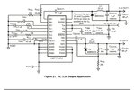
I like this chip and I will use it for my design. I have one issue though , the data sheet is not giving any board layout , how do I go about the pcb layout for this circuit?

LM2717-ADJ.jpg
 
Last edited:

Hi,

Have a go with this datasheet, might be more helpful:

https://www.ti.com.cn/cn/lit/ds/symlink/lm2717.pdf

Using RFb1 and RFb2 you calculate output voltage, or more accurately you get the value of RFb1 from a random-ish selection of value for RFb2 in a formula that includes the 5V out.

Doing a quick calculation for 5V out, I got RFb1 = 29,463 ohms if RFb2 = 10K. Hope that's right, looks a straightforward formula on page 8 of the above datasheet.

PCb layout... from what I know, best look well into converter design PCB layout app notes, seems a bit of a science, things like keeping some components away from others, very short tracks for some parts, and other aspects worthy of due consideration. I'll look for a datasheet for a similar device that actually explains it a little better and post it shortly.

- - - Updated - - -

The Micrel one is page 23, TI TPS55340 is page 26 and TI TPS54233-Q1 is page 17 for layout guidelines, even if last two are for the specific last two devices, basically all share same recommendations and are good for getting correct orientation and ideas for your circuit layout.

View attachment an-15 Practical Switching Regulator Circuits Micrel.pdf
View attachment tps54233-q1.pdf
View attachment tps55340.pdf


Probably easier way to calculate RFb1 for any RFb2 value you choose for "exactly" 5V, is:

multiply RFb2 by 2.9463299131807419100236779794791 (again, do check in case I made a mistake calculating it).
 
Hi,

Have a go with this datasheet, might be more helpful:

https://www.ti.com.cn/cn/lit/ds/symlink/lm2717.pdf

Using RFb1 and RFb2 you calculate output voltage, or more accurately you get the value of RFb1 from a random-ish selection of value for RFb2 in a formula that includes the 5V out.

Doing a quick calculation for 5V out, I got RFb1 = 29,463 ohms if RFb2 = 10K. Hope that's right, looks a straightforward formula on page 8 of the above datasheet.

PCb layout... from what I know, best look well into converter design PCB layout app notes, seems a bit of a science, things like keeping some components away from others, very short tracks for some parts, and other aspects worthy of due consideration. I'll look for a datasheet for a similar device that actually explains it a little better and post it shortly.

- - - Updated - - -

The Micrel one is page 23, TI TPS55340 is page 26 and TI TPS54233-Q1 is page 17 for layout guidelines, even if last two are for the specific last two devices, basically all share same recommendations and are good for getting correct orientation and ideas for your circuit layout.

View attachment 123790
View attachment 123791
View attachment 123792

can I just use the RFB values as suggested in the data sheet on page 17 ?

LM2717-ADJ.jpg

- - - Updated - - -

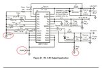
I m not understand what is AGND, PGND and the triangle symbol is in the circuit diagram , see the red circles in the diagram please
.LM2717-ADJ.jpg
 

Hi,

You can use the same values as datasheet suggests. there is no problem about it.

But , Please Check this : LM2717-adj is dual adjustable Regulator and LM2717 is Dual , but one fixed output as 3.3V and one adjustable output.

about PCB : you can check these documents. these are TI Evaluation boards for LM2717 & LM2717-adj

LM2717 Evaluation board : https://www.ti.com/lit/pdf/snva109

LM2717-adj Evaluation board : https://www.ti.com/lit/pdf/snva155
 

thanks Memarian for the Evalution board layout for LM2717.
my first hurdle ...the L1,L2 inductors they are suggesting is not available either at digi-key or at mouser 22 µH, DO3316P-223 . can you suggest an equivalent?
 

Hi,

Analog Ground and Power Ground, the other triangle is the same symbol as for analog ground. You'd need to find a reliable reference for what each ground symbol actually means, even if people use them interchangably for their circuits (we shouldn't really, but still, like earth isn't ground).

Not sure what they mean here with both grounds, as I think you have to tie them together in the same place somewhere on the PCB (or off it, depending on how you put it all together) to avoid ground loops. Analog circuitry likes a quiet supply, power (with inductors, etc. would be "noisy"). Could be like the split ground plane approach for mixed digital and analog circuits - some people don't bother, simple practice for that is to put digital return path(s) in middle of board and as close to their origin as possible, and analog all around rest where needed. If you have the luxury of a board with several planes: agnd, pgnd, +V power, signal, etc. then great..., if not a trick is to either design in a guard rail or if it's like my cheapo home-made boards cut a ... pseudo guard rail around noisy return paths and that way you do not need to split the ground plane which some consider worse than a single plane mixed signal board, but all that stuff is for professionals with real board design experience to comment on (as opposed to my probably zero-compliant home-made PCBs).

A guess is to tie the power grounds in that schematic at the same point to the power supply input negative terminal.

For the inductor, if you haven't found an alternative, look at companies like coilcraft's web, (or e.g. Murata or Vishay, perhaps - not sure 'tho) etc., or type the specific inductors qualities into manufacturer filters to find an alternative. RS-online may have what you need, and they have a pretty handy filter with multiple parameters to whittle choice down to a not overwhelming choice :). You're in the US - Jameco?
 

how about this one from digi-key ? 490-10840-1-ND
it has all the same specs as the original

also I have two questions :
1- The evaluation board is showing the following caps in BOM as "open" what does it mean?

CC3, CC4 Open
CSS1, CSS2 Open

2- what is SHDN1 and SHDN2 ? they are not connected in fig21 but I think they are being used in the evaluation board.
 
Last edited:

how about this one from digi-key ? 490-10840-1-ND
it has all the same specs as the original

also I have two questions :
1- The evaluation board is showing the following caps in BOM as "open" what does it mean?

CC3, CC4 Open
CSS1, CSS2 Open

2- what is SHDN1 and SHDN2 ? they are not connected in fig21 but I think they are being used in the evaluation board.

Hi,

About the Inductor that you suggested : 490-10840-1-ND has a saturation current=2A , which is low if you want to have 2A output. this should be higher. there is also no SRF in the datasheet.
I suggest one of these : 587-2002-1-ND or SRR1260-220MCT-ND or SRR1280-220MCT-ND or 587-2975-1-ND or 283-4083-1-ND or

you can check this link (You can find many inductors in that page which have good price and good specs.) :BTW, select and inductor with lower DC Resistance. you will have lower ripple in output. (this table shows you inductors with SRF > 10MHz, which is fine for your application)

https://www.digikey.com/product-search/en?pv66=162&pv66=767&pv66=212&pv66=77&pv66=2376&pv66=127&pv66=129&pv66=6&pv66=168&pv66=3202&pv66=287&pv66=131&pv66=2195&pv66=49&pv66=169&pv66=134&pv66=2404&pv66=2847&pv66=7&pv66=172&pv66=8&FV=fff40003%2Cfff80013%2Cc0003%2Cc0005%2Cc000e%2Cc0028%2Cc0150%2C4c000e%2C4c01ae%2C4c03bf%2C4c03d5%2C4c03e0%2C4c0955%2C4c09b9%2C4e8000d%2C4e80020%2C4e80021%2C4e8009c%2C4e8009d%2C4e8009e%2C4e8009f%2C4e800a0%2C4e800a5%2C4e800c7%2C4e80364%2C4e80367%2C4e80731%2C4e80758%2C4e807a2%2C4e807a4%2C4e80a9d%2C4e80bc3%2C4e80dd5%2C4e810c2%2C4e811dc%2C4e811e5%2C4e81228%2C4e81282%2C4e81301%2C4e81597%2C4e8177a%2Cb08003e%2Cb080045%2Cb080050%2Cb080051%2Cb08005a%2Cb08005b%2Cb080065%2Cb080067%2Cb08006d%2Cb08006e%2Cb08006f%2Cb080074%2Cb08029e%2Cb0802a3%2Cb08031e%2Cb08031f%2Cb080322%2Cb08032d%2Cb080338%2Cb0803b0%2Cb080439%2Cb080454%2C130c0001%2C130c0007%2C130c0009%2C130c0015%2C130c0017%2C130c002c%2C130c0062%2C130c0090%2C130c00a6%2C130c00b1%2C130c01a8%2C130c01ce%2C130c01f4%2C130c0207%2C130c0213%2C130c023e%2C130c0263%2C130c0271%2C130c02b1%2C130c02e2%2C130c030d%2C130c0349%2C130c0371%2C130c03a2%2C130c03db%2C130c0433%2C130c0458%2C130c0459%2C13180002%2C13180035&mnonly=0&newproducts=0&ColumnSort=0&page=1&quantity=0&ptm=0&fid=0&pageSize=25


about your questions :

1) CSS1 & CSS2 are for soft-start operation, if you don't need soft-start you can ignore them.
About CC3, CC4 : i didn't understand it fully yet , but i think they are required , if you want to use soft-start . it seems they are part of some compensation network for using in soft-start.

2) SHDN1 & SHDN2 are shutdown pins. They are Active low. you can shutdown the regulators independently, if you like. Leave it open for normal operation. (Page 2 of Datasheet)

Good Luck!
 
Last edited:
  • Like
Reactions: aliyesami

    V

    Points: 2
    Helpful Answer Positive Rating

    aliyesami

    Points: 2
    Helpful Answer Positive Rating
Hi,

About CC3, CC4 : i didn't understand it fully yet , but i think they are required , if you want to use soft-start . it seems they are part of some compensation network for using in soft-start.

Good Luck!

thanks for your recommendation, i chose SRR1260-220M as inductor.
I cant find CC3 and CC4 capacitors you are mentioning anywhere on the datasheet or on the evaluation board ?
 

Hi,

They're in snva109, on page 2 in the board layout image, they are labelled in the middle left-hand side block (above CC1 and below CC2), the Bill Of Materials on page 3 says "CC3, CC4: open".
 

Hi,

They're in snva109, on page 2 in the board layout image, they are labelled in the middle left-hand side block (above CC1 and below CC2), the Bill Of Materials on page 3 says "CC3, CC4: open".

yes i see them now , how can they not be in schematics then ? its confusing
 

...no idea, maybe as it's an evaluation board, and you can't know what components people will use, they leave multiple options open to the evaluater/user to use different sized components or to have different layouts or try ideas out using the free pins. A current shunt monitor evaluation board seemed to have these options, from SMD to leaded resistors.

Also, I read that good design practice for prototypes is to leave space for anything you may need to add after production (avoid whole board done again for sake of one capacitor/transistor), and to have a couple of footprints in case you find you need to change one "it's not working as predicted" component for another (e.g. change a TO-92 to a TO-220 or to a SOIC, and so on).

since CC3 and CC4 are not in schematics i will safely ignore them.

- - - Updated - - -

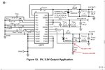
i am not understanding the role of RFB2, both its ends are on ground potential which is not making any sense to me.
please see the attached drawing.
LM2717.jpg
 

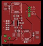
here is my schematics and board layout , do you see any issues? or any way i can improve it please let me know.
and this design is without using RFB2.

LM2717_schematics.jpg

LM2727_Board_layout.jpg
 

here is my schematics and board layout , do you see any issues? or any way i can improve it please let me know.
and this design is without using RFB2.

View attachment 123827

View attachment 123828

Hi,

There is a very important thing : You need RFB2 like the Original Schematic. The Node between Lower Pin of RFB1, Higher Pin Of RFB2 and FB2 Pin IS NOT GND. In the original schematic , lower end of RFB1 Crossed Over GND Node to RFB2. It's not connected to GND. if it was connected to GND , there was a Junction (those CIRCLES) Like the one between RFB1,RFB2 and the track to FB2 PIN. If you use it like this , your circuit won't work and i think your REG2 Output will be around input voltage.

Also i think it's better that you change RC1,CC1 & RC2,CC2 placement like the evaluation board , in series , not like a loop. (your electrical connection is correct , but you placement seems like a loop, this shouldn't be like this)

P.S : Hope it's not too late (and hopefully you didn't order your PCB ), It seems we live in different time zones.

Good Luck!
 
Last edited:

Status
Not open for further replies.

Part and Inventory Search

Welcome to EDABoard.com

Sponsor

Back
Top