Continue to Site

Welcome to EDAboard.com

Welcome to our site! EDAboard.com is an international Electronics Discussion Forum focused on EDA software, circuits, schematics, books, theory, papers, asic, pld, 8051, DSP, Network, RF, Analog Design, PCB, Service Manuals... and a whole lot more! To participate you need to register. Registration is free. Click here to register now.

[SOLVED] RF Power Amplifier Gain Not Flat.

Status
Not open for further replies.

kmmaran

Member level 1
Member level 1
Joined
May 16, 2005
Messages
41
Helped
2
Reputation
4
Reaction score
2
Trophy points
1,288
Activity points
1,596
RF Experts,

I am using PD55015E (model) from ST Micro. Using MWO I have matched the output for Max Power from Load pull simulation, and matched with input with parallel RC for stability. Everything went well, good PAE and Max Power, S11 is close to 50ohm, but the power gain is not flat as you can see from the pic, and P1dB is bumpy (no pic attached).

Can anyone explain why the gain is not flat, I try both in ADS and MWO, and both having the same problem.

Thank you for the help.
Manimaran Gain_Comp.JPG
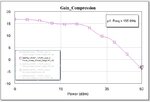
 

You could post de PAE evolution with Gain, just to check. But I think that is a normal behaviour, i.e., PA tend to reduce their gain when approaching their Peak Power. I do not know what class are you using, but from that characteristic I would say that it is a linear Amplifier. You should post more graphics and the schematic for more info.

With best regards.
 

dshoter13

Thank you for your reply. I will post the necessary plot asap.

But one question, the gain compression should be flat and not related to bias current or class of amplifier, is that correct.

BRgds
 

It depends. Depends of the Class of Operation. With the same transistor you will have different PUF ( Power Factor Utilization) depending on the class that the transistor is operating. But post those plots please.
 
dshoter13

I have attached the file for your advice, hope can explain from the plot and circuit for gain issue.

Brgds
Manimaran
 

Attachments

  • Design_Detail.rar
    268.2 KB · Views: 145

The name of the phenomenon is "gain expansion" and appears mainly in the power amplifiers biased in AB class.
The main reason is the improper output load impedance seen by the amplifier (drain choke inductor and the LPF in this case).
I see in the ST datasheet that they recommend to use a capacitor at the output (C10,C11), which you don't have in your schematic.
Drain choke value also could affect this behavior.
 
Dear vfone,

Thank you for your reply, I will go read about gain expansion and use your advice to look at the load impedance. Will come discuss further about my findings.

BRgds
Manimaran
 

vfone,

I have read a number of articles and pls verify my explanation is correct.
Basically, the gain expansion occur before the PA compresses. And the reason for Gain Expansion is because of the gain rises faster and expand before it compress. If the gain rises slow and steady than the expansion will not happened.

Other thing is, I have matched the PA for Max power, meaning the output load is correct and achieved max power , then where does this gain expansion came from?

Brgds
Manimaran
 

Probably because you are using a class AB. If you use class B you should not get gain expansion. I am not sure about this, but to verify that you only have to do some basic math with the Fourier Coefficientes of your drain's current waveform.

With best regards.
 
I think it should be on the order of 0.2dB and is believed to be the result of rectification of the RF on the gate of the FET changing the FET DC bias point.
 
Dear RF Experts,

Thank you very much for your time discussing the issue. Really appreciate you valuable information and I am on the process of solving the issue.

BRgds
Manimaran
 

Status
Not open for further replies.

Part and Inventory Search

Welcome to EDABoard.com

Sponsor

Back
Top