Continue to Site

Welcome to EDAboard.com

Welcome to our site! EDAboard.com is an international Electronics Discussion Forum focused on EDA software, circuits, schematics, books, theory, papers, asic, pld, 8051, DSP, Network, RF, Analog Design, PCB, Service Manuals... and a whole lot more! To participate you need to register. Registration is free. Click here to register now.

Genber file of a PCB with inside cut

Status
Not open for further replies.

piyush manavar

Member level 4
Member level 4
Joined
Jul 23, 2009
Messages
78
Helped
10
Reputation
20
Reaction score
8
Trophy points
1,288
Location
india
Activity points
1,827
Hi

Can any body help me to generate Gerber data for a pcb with some cutting work inside it. Like a square or circle cut inside the PCB not included edge. I have tried it with different layer but i am not able to regenerate for the same.

I have attached a pic of some inner cutting work. I just want to know in which layer this artwork have to include so which file should be given to manufacturer.
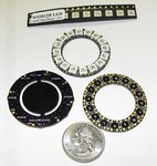
CustomNeoPixel131202c.jpg

Thanks
-Piyush
 

The usual way is to add internal contures to the outline layer. I think it's possible with any standard layout tool.
 
Hi FvM


I tried with different layers like dimension, drill, etc but manufactuarar said data is unsufficent. Also tried to view it in online gerber view but if cutting work is at edge then it works well even if you can put some notch or hall and it will be sown well but the same artwork with same layer inside pcb it not shown any hollow space inside PCB.

I am using eagle software..

-Piyush
 

For waste tabs, you must put microvias at edge or just outside inner circle for clean break on all layers.

You haven't done your thermal design properly with FR4 and microvias.
Suggest you use MCPCB.

240 mW x 16= 4W needs at least 16 sq. cm or 2cm²/W on MCPCB with torch handle heatsink or 4cm²/W without sink.

This is ~2.6cm²/W but 10x higher thermal resistance.

Layout & Enclosure thermal design will make a big difference on Tj rise. Which should be 40C rise for a good design or 60 deg rise for not so good, and 80 deg C rise for a terrible design.
 
I don't remember that I have tried or not with layer no 46 but definetry i will try and let you know.

Thanks
-Piyush
 

Hi FvM

I tried with layer no 46 but it is not working. I generate all gerber data and saw it with online 3d gerber view. It not sowing any cut in same layer except out line. I am here uploading my sample file here you can also try and let me know if i am doing wrong.

The square mentioned 9.8 x 63 mm is the inside cutting area.

Thanks
-Piyush
 

Attachments

  • Flex.zip
    83.3 KB · Views: 104

I looked at your files and and here's what I see:
Your .cam file does export the dimension layer on the silkscreen layers (the eagle CAM jobs that come with the software do this by default), but that means it's displayed along with any other silkscreen artwork. This is a problem when you have internal cuts, because the manufacturer will not be able to tell the difference between the silkscreen and the tooling paths you desire. See below:


So what you need to do is create a new layer in the CAM processor which contains only routing information. It doesn't really matter what layer you use to draw it in eagle (I use dimension).

Also your dimension layer has a single line on the right side, which I'm assuming is a mistake. In any case, the manufacturer won't like it.

Also you should draw your dimension layer using 0 line width.
 
I agree with mtwieg that you draw the cut out information on any layer if it's output separately in the postprocess. Layer 46 has no data at all.
 
There should be something like "board cutout" in Eagle as well, check out their manuals. In my CAD software there is a board cutout tool, I don't have to put cutouts on the another layer, since board polygon goes to Gerber with cutouts in it automatically. However if there is no such option in Eagle (I'm using DipTrace) make sure you communicate with a PCB house and use the separate layer for cutouts, one more for assembly information, dimensions e.t.c. Just look at the design like they will do.
Don't mix up contents between layers. Silkscreen is for silkscreen only and so on.
 
Status
Not open for further replies.

Part and Inventory Search

Welcome to EDABoard.com

Sponsor

Back
Top