Continue to Site

Welcome to EDAboard.com

Welcome to our site! EDAboard.com is an international Electronics Discussion Forum focused on EDA software, circuits, schematics, books, theory, papers, asic, pld, 8051, DSP, Network, RF, Analog Design, PCB, Service Manuals... and a whole lot more! To participate you need to register. Registration is free. Click here to register now.

snm calculation of sram array

Status
Not open for further replies.
hello
i want simulation sram in hspice
but i dont know
please please help me for netlist and calculate SNM
 

i want simulation sram in hspice
but i dont know
please please help me for netlist and calculate SNM

This is a 2-month old thread.Maybe better to start a new thread.

I used to do SRAM simulations in T-Spice.But do you have library files? & which length are you working on ?
Do you know about butterfly curves ?

A sample code on which you can work:

Code:
*[B]CODE-SPICE[/B]
.lib "E:\Stuff\NG Spice\SPICE PROGRAMS\BTP\45 nominal.md"

.GLOBAL VDD
.PARAM VDD=0.6V 
.options list post 
*.temp 100 

.PARAM U=0
.PARAM UL='-VDD/sqrt(2)' 
.PARAM UH='VDD/sqrt(2)' 
.PARAM BITCAP=1E-12

MPL QD QB VDD VDD PMOS W=45n L=45n AS=40.5f PS=1.89u AD=40.5f PD=1.89u
MNL QD QB GND GND NMOS W=90n L=45n AS=81f PS=1.98u AD=81f PD=1.98u  
MPR QBD Q VDD VDD PMOS W=50n L=45n AS=162f PS=2.16u AD=162f PD=2.16u  
MNR QBD Q GND GND NMOS W=90n L=45n AS=81f PS=1.98u AD=81f PD=1.98u 
MAL BLB WL QBD GND NMOS W=45n L=45n AS=40.5f PS=1.89u AD=40.5f PD=1.89u
MAR BL WL QD GND NMOS W=45n L=45n AS=40.5f PS=1.89u AD=40.5f PD=1.89u

VVDD VDD GND DC=VDD

*****Read****
*VWL WL GND PULSE(1 0 0n 1n 1n 30n 1200n) 
*.IC V(BL)=VDD
*.IC V(BLB)=VDD
*****Hold****
VWL WL GND DC=0v
.IC V(BL)=VDD
.IC V(BLB)=VDD
*****Write***
*VBL BL GND PULSE (0 1 0n 5n 5n 40n 100n)
*VBLB BLB GND PULSE (1 0 0n 5n 5n 40n 100n)
*VWL WL GND PULSE(0 1 0n 1n 1n 75n 200n)
CBLB BLB 0 BITCAP
CBL BL 0 BITCAP


EQ Q 0 VOL='1/sqrt(2)*U+1/sqrt(2)*V(V1)' 
EQB QB 0 VOL='-1/sqrt(2)*U+1/sqrt(2)*V(V2)'
EV1 V1 0 VOL=' U + sqrt(2)*V(QBD)'
EV2 V2 0 VOL='-U + sqrt(2)*V(QD)'
EVD VD 0 VOL='ABS(V(V1) - V(V2))'

.DC U UL UH 0.01
*.tran 0.5n 500n
*.PRINT DC V(QD) V(QBD) V(QB) V(Q) V(V1) V(V2)
.PRINT DC V(QB) V(QBD)
*.print tran V(BL) V(BLB)
.MEASURE DC MAXVD MAX V(VD)
.MEASURE DC SNM param='1/sqrt(2)*MAXVD'
.END
 
hello thanks alot.
i have 32nm technology
i am a student and i dont know working with hspice for butterfly curves.
excuse me
 
hi
i simulated this netlist and no error
but i dont know about it
 

hi
i simulated this netlist and no error
but i dont know about it

Did you change this line in the code that i posted :
.lib "E:\Stuff\NG Spice\SPICE PROGRAMS\BTP\45 nominal.md"
to the location on your pc where your 32 nm library file is located
So it would look like this:
.lib "..your library path..\library file name"
and also change the L=45n in the following lines to 32n:


Code dot - [expand]
1
2
3
4
5
6
MPL QD QB VDD VDD PMOS W=45n L=45n AS=40.5f PS=1.89u AD=40.5f PD=1.89u
MNL QD QB GND GND NMOS W=90n L=45n AS=81f PS=1.98u AD=81f PD=1.98u 
MPR QBD Q VDD VDD PMOS W=50n L=45n AS=162f PS=2.16u AD=162f PD=2.16u 
MNR QBD Q GND GND NMOS W=90n L=45n AS=81f PS=1.98u AD=81f PD=1.98u 
MAL BLB WL QBD GND NMOS W=45n L=45n AS=40.5f PS=1.89u AD=40.5f PD=1.89u
MAR BL WL QD GND NMOS W=45n L=45n AS=40.5f PS=1.89u AD=40.5f PD=1.89u


By don't know about it,do you mean not able to understand it ? Are you getting butterfly curves ?
Butterfly curves look like this:
 

Attachments

  • Butterfly_1V.JPG
    Butterfly_1V.JPG
    91.3 KB · Views: 232
Last edited by a moderator:

i simulated that netlist but can not see Butterfly curves in CosmosScope

- - - Updated - - -

for example in read operation read:
VWL WL GND PULSE(1 0 0n 1n 1n 30n 1200n)
.IC V(BL)=VDD
.IC V(BLB)=VDD
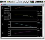
i see this picUntitled.jpg
 

Hi,

Did you see the waveform that i attached in post #7.You need to have v(QB) & v(QBD) in the same plot.

and in your post #6 you have mentioned the following code:

Code:
VWL WL GND PULSE(1 0 0n 1n 1n 30n 1200n) 
.IC V(BL)=VDD
.IC V(BLB)=VDD

If you've simulated exactly as per my code,you are driving WL from 1 to 0 & Vdd is only 0.6,so i suggest you to change the value of Vdd to 1 as well.

changes in my code:-
Code:
.GLOBAL VDD
.PARAM VDD=0.6V
 

hello
why ?
Code:
MPL QD QB VDD VDD PMOS 
MNL QD QB GND GND NMOS   
MPR QBD Q VDD VDD PMOS 
MNR QBD Q GND GND NMOS 
MAL BLB WL QBD GND NMOS 
MAR BL WL QD GND NMOS
if they are changing with :
Code:
mosn1              Q          QB            0                0         nmos      l=32n   w=90n
mosp2              Q          QB          vdd            vdd       pmos      l=32n   w=50n  
mosn3              QB        Q              0                0         nmos      l=32n   w=90n   
mosp4              QB        Q            vdd            vdd       pmos      l=32n   w=50n
mosn5              BL         WL           QB             0         nmos      l=37n   w=47n
mosn6              BLB       WL           Q               0         nmos      l=37n   w=47n
what happend??
 
Last edited by a moderator:

Hi samira,
if they are changing with :
Code:
mosn1              Q          QB            0                0         nmos      l=32n   w=90n
mosp2              Q          QB          vdd            vdd       pmos      l=32n   w=50n  
mosn3              QB        Q              0                0         nmos      l=32n   w=90n   
mosp4              QB        Q            vdd            vdd       pmos      l=32n   w=50n
mosn5              BL         WL           QB             0         nmos      l=37n   w=47n
mosn6              BLB       WL           Q               0         nmos      l=37n   w=47n
what happend??

Your pass transistors,why do they have a channel length of 37n,don't change the length,try only changing the width of transistors.You are using 32nm library,so keep length fixed at 32n
Also why does your code not have other mos parameters like area etc.. apart from length & width,like my code has.

Your pass transistors are also wrongly connected.Modify your code to the below code:
Code:
mosn1            Q         QB         0          0      nmos      l=32n   w=90n
mosp2            Q         QB       vdd         vdd   pmos      l=32n   w=45n  
mosn3            QB       Q          0           0      nmos      l=32n   w=90n   
mosp4            QB       Q         vdd         vdd  pmos      l=32n   w=50n
[B]mosn5        BLB     WL          QB          0         nmos      l=32n   w=32n
mosn6             BL       WL          Q            0         nmos      l=32n   w=32n [/B]

Now with the above code,plot Q & QB in same plot to get butterfly curve
 
helllo
excuse me for my alots question
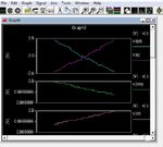
when i simulated in read mode i see:
Untitled1.jpg
 

helllo
excuse me for my alots question
when i simulated in read mode i see:
From your attached waveform,it seems you Vdd = 0.6 V,can you increase it to 1V & post the simulation waveform.
And can you do hold waveform also? I've seen from my simulations that you get better hold waveforms than read.

Most probably,your vdd = 0.6 is less than threshold voltage(vth =0.7) ? are you looking for sub-threshold operation ?
 

hi
when we explanation noise voltage source for read and write operation??
 

hi
when we explanation noise voltage source for read and write operation??
What do you mean ? I can't understand what you're saying.

Did you do the changes i suggested in post #13,by changing Vdd from 0.6 V to 1 V ? Are you doing sub-threshold design ?
 

hello
why HOLD SNM and WRITE SNM are similar???
HOLD SNM = 0.2242
READ SNM = 0.1358
WRITE SNM = 0.2243

please help me please.
 

    Prashil@03

    Points: 2
    Helpful Answer Positive Rating
Status
Not open for further replies.

Similar threads

Part and Inventory Search

Welcome to EDABoard.com

Sponsor

Back
Top