Continue to Site

Welcome to EDAboard.com

Welcome to our site! EDAboard.com is an international Electronics Discussion Forum focused on EDA software, circuits, schematics, books, theory, papers, asic, pld, 8051, DSP, Network, RF, Analog Design, PCB, Service Manuals... and a whole lot more! To participate you need to register. Registration is free. Click here to register now.

what is difference between Structural, behavior and test bench in VHDL

Status
Not open for further replies.

Arrowspace

Banned
Full Member level 3
Joined
Jan 23, 2015
Messages
186
Helped
3
Reputation
6
Reaction score
3
Trophy points
18
Activity points
0
what is difference between Structural, behavior and test bench in VHDL?
 

test bench is defining the stimuli for your code.
where as structural and behavioral are different types of modelling your code
 
Can i do transistor level modelling in VHDL
 

i have done it using verilog. i think it is possible with vhdl also
 

Can you provide me sample code for transistor level modeling ?

I am getting an error in VHDL code Test beach simulation. I have attached Pic for it.
 

Attachments

  • 3.JPG
    3.JPG
    136 KB · Views: 209

Your CLA_Addr instance is incomplete, it ends on the line cout => cout, where is the closing );?

For a 4-bit shift register...
Structural modeling:

Code VHDL - [expand]
1
2
3
4
5
6
7
8
9
10
11
12
13
14
15
16
17
18
19
20
21
22
23
24
25
26
27
signal clk : std_logic;
signal shift_in  : std_logic;
signal shift_reg : std_logic_vector(3 downto 0);
-- assuming the existance of a d FF component
s0 : dff port map (
  d => shift_in,
  q => shift_reg(0),
  c => clk
);
 
s1 : dff port map (
  d => shift_reg(0),
  q => shift_reg(1),
  c => clk
);
 
s2 : dff port map (
  d => shift_reg(1),
  q => shift_reg(2),
  c => clk
);
 
s3 : dff port map (
  d => shift_reg(2),
  q => shift_reg(3),
  c => clk
);


For behavioral modeling:

Code VHDL - [expand]
1
2
3
4
5
6
7
signal clk : std_logic;
signal shift_in  : std_logic;
signal shift_reg : std_logic_vector(3 downto 0);
process (clk)
begin
  shift_reg <= shift_reg(2 downto 0) & shift_in;
end process


Now which way is easier to see what is being implemented?


Can i do transistor level modelling in VHDL
i have done it using verilog. i think it is possible with vhdl also
Not sure this is as easy to do in VHDL. Verilog was designed to model transistor level logic. It includes as part of the language nmos, pmos, cmos, etc. It also supports 8 levels of drive strength from high impedance...to supply rail. I imagine by now someone has written a package that tries to address some of this for VHDL.
 

Your CLA_Addr instance is incomplete, it ends on the line cout => cout, where is the closing );?

For a 4-bit shift register...
Structural modeling:

Code VHDL - [expand]
1
2
3
4
5
6
7
8
9
10
11
12
13
14
15
16
17
18
19
20
21
22
23
24
25
26
27
signal clk : std_logic;
signal shift_in  : std_logic;
signal shift_reg : std_logic_vector(3 downto 0);
-- assuming the existance of a d FF component
s0 : dff port map (
  d => shift_in,
  q => shift_reg(0),
  c => clk
);
 
s1 : dff port map (
  d => shift_reg(0),
  q => shift_reg(1),
  c => clk
);
 
s2 : dff port map (
  d => shift_reg(1),
  q => shift_reg(2),
  c => clk
);
 
s3 : dff port map (
  d => shift_reg(2),
  q => shift_reg(3),
  c => clk
);


For behavioral modeling:

Code VHDL - [expand]
1
2
3
4
5
6
7
signal clk : std_logic;
signal shift_in  : std_logic;
signal shift_reg : std_logic_vector(3 downto 0);
process (clk)
begin
  shift_reg <= shift_reg(2 downto 0) & shift_in;
end process


Now which way is easier to see what is being implemented?


Not sure this is as easy to do in VHDL. Verilog was designed to model transistor level logic. It includes as part of the language nmos, pmos, cmos, etc. It also supports 8 levels of drive strength from high impedance...to supply rail. I imagine by now someone has written a package that tries to address some of this for VHDL.


After putting closing I am getting this error.

- - - Updated - - -

This is my code for test bench


Code VHDL - [expand]
1
2
3
4
5
6
7
8
9
10
11
12
13
14
15
16
17
18
19
20
21
22
23
24
25
26
27
28
29
30
31
32
33
34
35
36
37
38
39
40
41
42
43
44
45
46
47
48
49
50
51
52
-- TestBench Template 
 
  LIBRARY ieee;
  USE ieee.std_logic_1164.ALL;
  USE ieee.numeric_std.ALL;
  USE ieee.std_logic_unsigned.all;
 
  ENTITY CLA_Adder_tb IS
  END CLA_Adder_tb;
 
  ARCHITECTURE behavior OF CLA_Adder_tb IS 
 
  -- Component Declaration
          COMPONENT CLA_Adder
             
          PORT ( a, b: IN STD_LOGIC_VECTOR (3 DOWNTO 0);
                 cin: IN STD_LOGIC;
                 s: OUT STD_LOGIC_VECTOR (3 DOWNTO 0);
                 cout: OUT STD_LOGIC
                    );
                      
          END COMPONENT;
 
          SIGNAL a, b: STD_LOGIC_VECTOR (3 DOWNTO 0) ;
          SIGNAL cin: STD_LOGIC;
          SIGNAL s: STD_LOGIC_VECTOR (3 DOWNTO 0);
             SIGNAL cout: STD_LOGIC;
             -- Clock period definitions
          constant clk_period : time := 1 ns;
 
  BEGIN
 
  -- Component Instantiation
          uut: CLA_Adder PORT MAP(
                 a  => a,
                      b  => b,
                 cin => cin,
                 s => s,
                 cout => cout);


               -- Clock process definitions( clock with 50% duty cycle is generated here
   clk_process :process
   begin
        clk <= '0';
        wait for clk_period/2;  --for 0.5 ns signal is '0'.
        clk <= '1';
        wait for clk_period/2;  --for next 0.5 ns signal is '1'.
   end process;
 
  END;


5.JPG
 
Last edited:

You never declared the clk signal. It's required that you declare everything before first using it.

BTW, your testbench doesn't apply any stimulus to the UUT inputs a, b, and cin?
 

You havent defined the clk signal
signal clk : std_logic;

Structual modelling : think of it like placing bits on a circuit board.
RTL Modelling (or behavioural) : using templates that will synthesise to digital logic components
behaviour modelling: could also include code that is completly unsynthesisable - like a bus functional model
testbench : something to test a design in (may use a mixture of all 3 types above)

VHDL does have 9 types for std_logic
U (uninitialised),
X(unkown - when you drive 0 and 1 together),
0,
1,
Z (high impedance),
H (weak high),
L (weak low),
W (weak unknown - driving H and L together),
- (dont care)

You probably can do transistor level modelling using these, but you cant use absolute voltage levels. You probably want VHDL-AMS for that
 
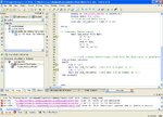
Ok , my problem get solve , but new problem with that I want to calculate time consume by adder to perform full task , but my simulation window always showing 1us and multiple of 1us
 

Attachments

  • 6.JPG
    6.JPG
    117.4 KB · Views: 160

Ok , my problem get solve , but new problem with that I want to calculate time consume by adder to perform full task , but my simulation window always showing 1us and multiple of 1us
What are you expecting? And how do you propose to calculate the time it takes to perform an add with combinational logic in a functional simulation? Any timing delays in the code aren't synthesizable nor are they representative of the actual implemented design timing.

You haven't supplied an input to cin and you are trying to run the simulation with a 1 GHz (1 ns period, i.e. 1000 ps) clock input, which explains why the clock signal is aliased in the display.

If you have a supply of FPGAs that can run useful logic at 1 GHz, then I'd like to know about that part, I have trouble getting them to meet timing at 350 MHz.
 

I want to calculate time consume by my adder to complete total task using simulation process. What I have do for actual implementation of adder.

What I have to do for reduction or increasing simulation speed.

- - - Updated - - -

I am getting this new error while changing timing of simulator
 

Attachments

  • 7.JPG
    7.JPG
    152.6 KB · Views: 188

There is no such thing as "time_precision" in VHDL. VHDL is event based, so everything occurs in delta cycles. A delta is an infinitely small amount of time. So in simulation, your addition will occur instantaneously, unless you simulate a gate level netlist.

There is absolutely no point in using simulation to "time" your adder, or any other logic, because delays in the FPGA are modified by 4 things: place and routing, process, voltage and temperature (PVT).
All 4 of these things affect the delay through your adder. So it is useless trying to get timing for it.

Much much better to put a register on each side of the adder and use timing analysis to see the delay from register to register (that will give you the "delay" you are looking for.
 

I want to calculate time consume by my adder to complete total task using simulation process. What I have do for actual implementation of adder. Please someone help me.
 

You cannot do that. The timing analyser can tell you all the delays, register to register, in your design.

What your are trying to do is fairly useless, as it can vary over time on a real chip.
 

Status
Not open for further replies.

Part and Inventory Search

Welcome to EDABoard.com

Sponsor

Back
Top