mahdiiust
Junior Member level 1

Hi
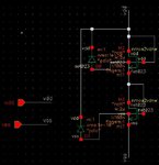
I must connect source and body terminals of all transistor to each other to obtain proper result in hspice.
but when i draw the layout i encountered a problem.
for pmos transistor it's ok because pmos transistors are in seperate wells and i can connect source and body to each other.
but for nmos transistor it's not! :-?
for those nmos transistors which their sources are not connected to Vss, the body is connected to Vss becuase all nmos transistors are in psub.
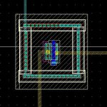
to solve this problem I try to isolate nmos from psub using nmosdnw transistors. but unfortunately the LVS isn't pass.
is there any important notice in using nmosdnw?I use TSMC0.18rf technology. can somebody help me?
thanks


