Continue to Site

Welcome to EDAboard.com

Welcome to our site! EDAboard.com is an international Electronics Discussion Forum focused on EDA software, circuits, schematics, books, theory, papers, asic, pld, 8051, DSP, Network, RF, Analog Design, PCB, Service Manuals... and a whole lot more! To participate you need to register. Registration is free. Click here to register now.

Shallow Trench Isolation

Status
Not open for further replies.

VLSI Bravo

Junior Member level 3
Joined
Mar 26, 2014
Messages
27
Helped
1
Reputation
2
Reaction score
1
Trophy points
3
Activity points
148
Hi all,
can any one explain why nmos current will decrease and Pmos current will increase in shallow trench isolation. pls explain STI effect in detail.

thanks in advance.
 

Hi VLSI Bravo

Not sure your question is clear: are you talking about STI stress effect or some think else?
 

hi dgnani,
i am talking about STI effects only, in depth........
 

STI stress effect can be described by two graphics parameters: SA, SB.They said on both sides of the gate to the active area on the edge of the distance. Mosfets characteristic parameters such as Vt, gm, Idsat,they will change with the following function into a linear:
Stress=1/((SA+0.5*L)+1/SB+0.5*L))

when high VGS, pMOS current will increase due to the reduce of Sa, but the nMOS current will decrease on on the contrary.

maybe the answer will help you.


your answer is not clear.........
 

STI creates silicon strain. Silicon strain alters mobility, and
differently so for electrons vs holes (a given strain tends to
favor one and hurt the other). Because strain is localized,
you will also see W-dependence especially as you come up
from minimum.

STI is also an inferior quality oxide, its fill can be a mysterious
floating gate and the trench can be an edge leakage factor.
A pair of small parallel parasitic MOSFETs in essence, but
with much poorer subthreshold slope / surface-states density
and a VT that you hope (but should not assume, especially in
unusual environments) is and remains well out of play (can
be HCI charged, radiation-shifted, etc.)
 
Stress=1/((SA+0.5*L)+1/SB+0.5*L))

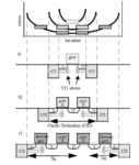
L refers to the gate length , therefore, only when SA, SB are being bigger, the stress will be smaller.See the fig. below, stress depends on a source area size, MOS tube in the position of the active region and MOS tube size :

1.png

the fig. above shows that increase the device to the active area on the edge of the distance can reduce the STI profit effect, so you need to add dummy in need of protection device, and the dummy must be Shared with protected device has a source area, otherwise is invalid.

In addition, due to the biaxial stress increased the hole mobility, reduced the electron mobility, therefore, with the decrease of the gate source voltage and source of PMOS transistor leakage current increase, and NMOS leakage source current is reduced, and the smaller the SA, SB, the more obvious effect.For very small gate voltage, NMOS source of leakage current will increase suddenly, especially in SA, SB when I was a child, this is the result of threshold value changes, the changes in source region is enhanced by stress/suppression system.

maybe the answer will help you.:smile:
 
Due to the different thermal expansion coefficients between Si and STI, there
exists biaxial compressive residual stress in the active region after processing.
STI-stress generally increases PMOS current and decreases NMOS current.
Stress relaxes exponentially with increased distance from Si/STI boundary.

Stress=1/((SA+0.5*L)+1/SB+0.5*L))

biaxial stress increased the hole mobility, reduced the electron mobility, therefore, :

Is this true always?.
Do you have any formula,scientific explanation for the above statement.
 
Last edited:

I have only a superficial knowledge of the subject. if u are interesting in it , you could find some academic paper to a in-depth study,as we known,many experts learn it nowadays.maybe u will find more answers

Good luck!
 

I have only a superficial knowledge of the subject. if u are interesting in it , you could find some academic paper to a in-depth study,as we known,many experts learn it nowadays.maybe u will find more answers

Good luck!

pls dont post text book answers here, post the answer if u know it clearly.

thanks & regards.
 

pls dont post text book answers here, post the answer if u know it clearly.

thanks & regards.

hi,VISI Bravo,
i am so sorry ,there must be some misunderstanding.i means what i know about STI is limited,and if any one wants to know more,what i can do is suggesting him to learn or study.the answers i reply above is not just the book answers,i just reply the theory that i know for and i think it at less can explain your question in this thread clearly and i hope it can help u.thanks!

sincerely
 
  • Like
Reactions: FvM

    FvM

    Points: 2
    Helpful Answer Positive Rating
hi,VISI Bravo,
i am so sorry ,there must be some misunderstanding.i means what i know about STI is limited,and if any one wants to know more,what i can do is suggesting him to learn or study.the answers i reply above is not just the book answers,i just reply the theory that i know for and i think it at less can explain your question in this thread clearly and i hope it can help u.thanks!

sincerely

thats ok .....
 

Status
Not open for further replies.

Part and Inventory Search

Welcome to EDABoard.com

Sponsor

Back
Top