Continue to Site

Welcome to EDAboard.com

Welcome to our site! EDAboard.com is an international Electronics Discussion Forum focused on EDA software, circuits, schematics, books, theory, papers, asic, pld, 8051, DSP, Network, RF, Analog Design, PCB, Service Manuals... and a whole lot more! To participate you need to register. Registration is free. Click here to register now.

Help with modify VIA in Allgero PCB editor!

Status
Not open for further replies.

lemta

Newbie level 4
Joined
Nov 16, 2010
Messages
6
Helped
0
Reputation
0
Reaction score
0
Trophy points
1,281
Activity points
1,317
Hi,
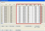
I have copied VIA default in database then modify drill size and pad size and save as with new name, but when use it seems to does not show drill hole (figure below, blue rectangle)

via.jpg

Any help? Thanks so much!
 

hi,
you have to call the path of via setup-->user preference-->library-->pad path and psm path after that add in constraint manager in physical constraint.
 

I have tried setup but still does't not show drill symbol, can you send me the file which make via with drill 0.5mm and diameter 1mm?
 

Hi
check the attached via details and bring it in design as i mention in above procedure
 

Attachments

  • pad40d20.rar
    672 bytes · Views: 69

Hi Kabaleevisu,
I have replaced current via with your but still does not show drill (it like via in blue rectangle, I want to it shown as via on the left.
via.jpg
I have sent you my via file (drill 0.5mm and size 1mm). I can't to know what is wrong :(
 

Attachments

  • via_drill20.rar
    4.7 KB · Views: 75

Hi,
Manufacturer-->NC-->Drill customization as shown in picture change the value you come to know,is it drill is available are not or else setup-->design parameter in that Display tab choose Display plated holes and padless holes it will show the drill point
 

Attachments

  • untitled.JPG
    untitled.JPG
    112.6 KB · Views: 101
  • Like
Reactions: lemta

    lemta

    Points: 2
    Helpful Answer Positive Rating
Hi,
Now I can see it, thank you :), also I'm not sure about the feature that: when I have clicked on component in layout plus , orcad capture will focus it on screen, but with pcb editor it do nothing?
 

Status
Not open for further replies.

Part and Inventory Search

Welcome to EDABoard.com

Sponsor

Back
Top