Continue to Site

Welcome to EDAboard.com

Welcome to our site! EDAboard.com is an international Electronics Discussion Forum focused on EDA software, circuits, schematics, books, theory, papers, asic, pld, 8051, DSP, Network, RF, Analog Design, PCB, Service Manuals... and a whole lot more! To participate you need to register. Registration is free. Click here to register now.

Soldering homemade double-sided PCB without through-pladed pads? Ideas?

Status
Not open for further replies.

neazoi

Advanced Member level 6
Joined
Jan 5, 2008
Messages
4,155
Helped
13
Reputation
26
Reaction score
15
Trophy points
1,318
Location
Greece
Activity points
37,164
Hello, I use the "sandwitched" photochemical teghnique to make double sided PCBs at home. After the PCBs are made, both upper and lower layers must be joined in some points (eg IC sockets).

Joining these points (if no plated-through is done) can be done using wires on single joins.
Or using the better quality IC sockets that extend their pins so they can be soldered on both sides.

In some cases soldering both sides cannot be done, for example on ISA bus connectors, since these components do not extend their pins too much out of the PCB.

What can be done to join the upper and lower layers in these cases without using plated-through?

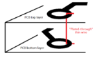
The only way I can think of, is passing through the hole a very fine wire and solder it on both layers, but without filling out the hole with solder. Prior to soldering the wire, bend it on both sides, so that it cannot pulled out of the hole. Then place in the component and solder it on the bottom side only. The thin wire acts as a plated-through then. Has anyone tried it?

Any other ways you can think of?
 
Last edited:

solder the short pin items on the board then do the others after assembling the 2 boards with suitable spacer?
I cant say I've heard of this before but why not if the components fit...
 
  • Like
Reactions: neazoi

    neazoi

    Points: 2
    Helpful Answer Positive Rating
solder the short pin items on the board then do the others after assembling the 2 boards with suitable spacer?
I cant say I've heard of this before but why not if the components fit...

Yes using spacers is one way, but not always feasible. This is because in some components (for example in ISA sockets on a motherboard) height alterations from the PBC is not an acceptable option. That is why I have thought of the thin wire solution, to create a custom plated-through. I believe if a thin wire is used there will be not much of a problem, since the hard to solder components (like the ISA bus sockets) do not have cilindrical pins but flat. The thin wire should be placed into the hole, where the flat surface of the component pin exists.

I have drawn a picture to see that I mean. I cannot think of any other solution?
 

Attachments

  • pcbds.png
    pcbds.png
    16.8 KB · Views: 159

neazo, good idea, I would only add, make sure that the wire is much longer then need be on the insertion side of the board, so the act of inserting a component, while still pulling the wire through, still leaves enough to play with on both sides of the board, Try to solder the wire along a track and not across a land, it easier that way.
Frank
 
  • Like
Reactions: neazoi

    neazoi

    Points: 2
    Helpful Answer Positive Rating
neazo, good idea, I would only add, make sure that the wire is much longer then need be on the insertion side of the board, so the act of inserting a component, while still pulling the wire through, still leaves enough to play with on both sides of the board, Try to solder the wire along a track and not across a land, it easier that way.
Frank

No I was thinking of presoldering the wire at the edges of the hole, but take care not to fill the hole with solder, so that the component pin can get through. Then I will place the component and solder it only on the bottom layer.


Clearly, one can use a variety of techniques to join the sides, as described.

As I understand the situation you describe, you have a hidden solder connection. What I do is solder first on the component side with the component just enough off the board to get the fine tip to the joints. Be sure there is adequate solder. Then heat the component's legs and re-seat it to be flush with the board. Resolder on the back side as usual. I have done 4-terminal components (e.g., bridge rectifiers) that way with a regular soldering iron. For more than 4 legs, you probably need a hot air or other type of device for heating multiple legs simultaneously.

John
 
  • Like
Reactions: neazoi

    neazoi

    Points: 2
    Helpful Answer Positive Rating
If your boards are back to back you're going to have raised solder face to face so you need some sort
of spacer no matter what you do - unless I've missunderstood how you plan to put the boards together.
On the other hand a main and daughter board connected via plugs may work?
 
  • Like
Reactions: neazoi

    neazoi

    Points: 2
    Helpful Answer Positive Rating
Clearly, one can use a variety of techniques to join the sides, as described.

As I understand the situation you describe, you have a hidden solder connection. What I do is solder first on the component side with the component just enough off the board to get the fine tip to the joints. Be sure there is adequate solder. Then heat the component's legs and re-seat it to be flush with the board. Resolder on the back side as usual. I have done 4-terminal components (e.g., bridge rectifiers) that way with a regular soldering iron. For more than 4 legs, you probably need a hot air or other type of device for heating multiple legs simultaneously.

John

I basically focus on "mostly" hidden top layer joins like shown in this picture http://www.ahmetozkurt.net/comporg/ekonomi/hw2006/tarik/Resim1.gif Reading at your message I am thinking of another way as well. if the top layer component pins are not so hidden, but hidden enough so that the iron cannot slip on them, then I could heat the component pin from the bottom side and touch a fine diameter solder wire onto the component pin on the top side. The heat on the component lead will melt the fine solder on the top side. Because the fine solder is small in diameter it can access the top part of the component pin. How does it sound?
 

How does it sound?

Sounds good to me. It is not much different than using solder paste and/or reflow with SMD components.

Of course, it is not very suited for automated assembly, but for homemade boards, it works fine.

John
 
  • Like
Reactions: neazoi

    neazoi

    Points: 2
    Helpful Answer Positive Rating
Sounds good to me. It is not much different than using solder paste and/or reflow with SMD components.

Of course, it is not very suited for automated assembly, but for homemade boards, it works fine.

John
This idea basically uses the component leads as hot soldering pins. Well, form theory to practice there may be problems with this idea though. for example I notice that the pins on the ISA bus sockets are really under the socket. On an ISA motherboard, the ISA sockets are too close together for even seeing the pins, imagine to try to solder them.

I believe the wire method described earlier is more convenient, although more time consuming. The only thing that worries me about this first method, is the mechanical stability, since now the components are only soldered to the bottom layer. For chips it is ok but for ISA BUS sockets it may be an issue when pressing the ISA cards to fit them.

Do you think that if I use lots of flux, it will be able to drive the solder through the component pin on the hole, at the opposite layer as well?
 

Status
Not open for further replies.

Similar threads

Part and Inventory Search

Welcome to EDABoard.com

Sponsor

Back
Top