Continue to Site

Welcome to EDAboard.com

Welcome to our site! EDAboard.com is an international Electronics Discussion Forum focused on EDA software, circuits, schematics, books, theory, papers, asic, pld, 8051, DSP, Network, RF, Analog Design, PCB, Service Manuals... and a whole lot more! To participate you need to register. Registration is free. Click here to register now.

Need Help for about room property in Altium designer ??

Status
Not open for further replies.

kabaleevisu

Advanced Member level 2
Joined
Apr 14, 2010
Messages
616
Helped
85
Reputation
170
Reaction score
81
Trophy points
1,308
Location
Chennai,India
Activity points
4,512
Hi everyone,
right now i am migrated into altium designer.i did small schematic and import in altium layout.let me know follow detail from altium designer.
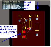
1.while import components are assign as room property is it need ??if multiple of sheet is available that time what i have to do is i need to keep in board workspace ??
2.how to make the origin for board outline ??
3.how to assign the origin while importing DXF in altium ?
please reply any one for this queries .......
 

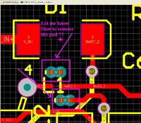
let me know how to remove the pad i could not know how to remove the pad ??
how to generate drill chart in altium
 

Hi Dear,

I can only tell you the following.

On the first hand, you can delete the rooms at all, but if you get use to with Rooms, these are very useful during your design.

If you use Hierarchical design methodology and repeat a single sheet many times (in form of sheet symbols) you will get an individual room for each sheet symbol. For example, if you are using a sheet five times as sheet symbols, you will get five rooms with all components in each room, now you have to place and route components of any single room and then you can "COPY ROOM FORMAT" to rest of the four rooms.

My text is just a hint, practice it an d you will have more understanding with some more questions hopefully.

Hi everyone,
right now i am migrated into altium designer.i did small schematic and import in altium layout.let me know follow detail from altium designer.
1.while import components are assign as room property is it need ??if multiple of sheet is available that time what i have to do is i need to keep in board workspace ??
2.how to make the origin for board outline ??
3.how to assign the origin while importing DXF in altium ?
please reply any one for this queries .......

- - - Updated - - -

let me know how to remove the pad i could not know how to remove the pad ??
how to generate drill chart in altium

I am using Altium Summer 09.

Place a Text on Drill Drawing Layer, change the text to .Legend by selecting from drop down menu in text properties. Now when you will Generate a gerber, a drill table will be generated on Drill Drawing Layer.

Hope it answer the question dear
 

Hi Maqbool,
Thanks for your comment and For example i am using 5 sheet for that 5 room will create in my design right.shall i place the component with in this room or shall i shift the group of component in room into another room,??
please post the suggest answer for second Quires
 

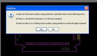
The error is shown because the lines you have selected to define board shape doesnot form an enclosed area. Check the link **broken link removed**
 
By default, altium places the components from one schematic sheet inside a room. The DRC shows an error if its placed outside. But we can change the room settings to " place components outside the room" which allows to place the room components outside that room and shows DRC error when tried to place inside.
Normally, i dont work with rooms and i think its needed only in highly complex designs.

To set the origin, run " Edit»Origin»Set " and select the point to be set as origin.Shortcut is E»O»S

To place a drill chart, there are 2 ways. You can place it directly by " Place»Drill Table"
Or you can place text anywhere on the sheet as ".legend" and this text will be replaced by the drill table in the gerbers.( In the pcb file, it will be visible as .legend only)

And about deleting the pad, what is the problem you face? You can delete the entire footprint of the particular component. Or if you want to delete only a specific pad in a footprint, take the component properties and uncheck the 'lock primitives' option which gives us access to individual pads or lines or whatever in a footprint and then modify or delete them as you like.

- - - Updated - - -

dear kabaleevisu,
About you board shape error, its shown because the lines selected by you in the DXF file to define the shape doesnot form an enclosed area. Select all the lines in the DXF so that the area is closed and then try 'Define board shape from selected objects' command
 
Dear Kapil.

Sorry fot late reply.

Altium Designer will make automatically a single room for each single sheet.

If there are 3 sheets, there will be 3 rooms... all the components will lie inside their corresponding room... you don't need to drag components to any room.

And Many Congratulations for the T20 Semifinal..... Best of Luck.

Regards,
Maqbool

Hi Maqbool,
Thanks for your comment and For example i am using 5 sheet for that 5 room will create in my design right.shall i place the component with in this room or shall i shift the group of component in room into another room,??
please post the suggest answer for second Quires

- - - Updated - - -

In Altium Designer Summer 09, I am unable to file PLACE>>DRILL TABLE.....
see the attached Picture

DDDDDD.png

By default, altium places the components from one schematic sheet inside a room. The DRC shows an error if its placed outside. But we can change the room settings to " place components outside the room" which allows to place the room components outside that room and shows DRC error when tried to place inside.
Normally, i dont work with rooms and i think its needed only in highly complex designs.

To set the origin, run " Edit»Origin»Set " and select the point to be set as origin.Shortcut is E»O»S

To place a drill chart, there are 2 ways. You can place it directly by " Place»Drill Table"
Or you can place text anywhere on the sheet as ".legend" and this text will be replaced by the drill table in the gerbers.( In the pcb file, it will be visible as .legend only)

And about deleting the pad, what is the problem you face? You can delete the entire footprint of the particular component. Or if you want to delete only a specific pad in a footprint, take the component properties and uncheck the 'lock primitives' option which gives us access to individual pads or lines or whatever in a footprint and then modify or delete them as you like.

- - - Updated - - -

dear kabaleevisu,
About you board shape error, its shown because the lines selected by you in the DXF file to define the shape doesnot form an enclosed area. Select all the lines in the DXF so that the area is closed and then try 'Define board shape from selected objects' command
 

Status
Not open for further replies.

Part and Inventory Search

Welcome to EDABoard.com

Sponsor

Back
Top