Continue to Site

Welcome to EDAboard.com

Welcome to our site! EDAboard.com is an international Electronics Discussion Forum focused on EDA software, circuits, schematics, books, theory, papers, asic, pld, 8051, DSP, Network, RF, Analog Design, PCB, Service Manuals... and a whole lot more! To participate you need to register. Registration is free. Click here to register now.

[SOLVED] Fast switching problem

Status
Not open for further replies.

alzomor

Advanced Member level 2
Joined
Jun 9, 2005
Messages
674
Helped
39
Reputation
78
Reaction score
8
Trophy points
1,298
Location
Germany
Activity points
6,406
Hi

I am trying to switch current in load using low side switching through controlled voltage into hi precision resistor in series with the load
1st I used a pnp transistor "FMMT593" for switching the problem was hi rise and fall time at low current of 50uA
snap shoot is shown in attachment aaaaaa10.bmp

Then I used a P channel mosfet instead DMP3098L it has a very good rise and fall time but have a very hi glitch with the rise edge.
as shown in aaaaaa03.bmp

Is there any suggestions for a transistor BJT or FET with good rise and fall time and no glitches.
or guidlines to overcome these two problems.

Regards
Hossam Alzomor
 

Attachments

  • aaaaaa10.bmp
    146.3 KB · Views: 103
  • aaaaaa03.bmp
    146.3 KB · Views: 106

The glitch is not the fault of the MOSFET, but with the circuit in which you use it. Post your circuit.
 

If the problem is not from the Mosfet why the glitches appears only with the Mosfet and disappear with the BJT?
any way you can find the circuit attached
Capture.JPG
Q4 is the switching transistor
for low current values VCC is 9 Volts
 

The problem is the relatively slow darlington and op amp regulator that supplies the switching transistor. This regulator cannot respond instantly to the change in load current, so when the switch turns on, the current is initially too high.

The glitches are not there with the BJT because that device is slow enough that the regulator can adapt as the BJT is slowly turning on.
 
Last edited:

I am little bit confused
If the problem is that the op amp and darlington are slow , then the current will start low and increase slowly, not the inverse.
am I right?
my problem Is that I get a high glitch when the Mosfet turns on.
this problem appears at low current values.
for high current values the glitch disappears.
if the problem is due to the speed of the op amp and darlington , so the glitch should be bigger for higher current.
you can check the attached pics in the 1st post above aaaaaa03.bmp .
 

When Q4 is off, the regulator is supplying zero current. When Q4 turns on, the regulator has to switch from supplying zero current to supply whatever current the load resistor calls for. In order to maintain a constant voltage output, the regulator has to switch from having the darlington almost fully off to having the darlington conducting. This calls for a different base drive from the op amp. The op amp is not able to change the base drive to the darlington instantly. When Q4 turns on, initially the output voltage from the regulator will drop. This will cause the existing base drive from the op amp to be much higher than the emitter, which will turn on the darlington hard. This will in turn make the output voltage spike upward. The feedback loop in the regulator circuit has to settle to new operating conditions in an effort to maintain the same output voltage. This is a general problem in all voltage regulated power supplies. It is called "load regulation" and it a dynamic component as well as a static component, as you have observed.

You may be able to fix the problem by putting a large capacitor between the emitter of Q4 and ground. This will supply the instantaneous current needed when Q4 turns on without suddenly upsetting the regulator.

As for why you don't see the problem with large currents, it could be that the feedback gain in that operating condition is less because the darlington is almost saturated.

On second thought, the capacitor might further destabilize the loop. Try putting a resistor between the emitter of Q4 and ground instead. That will ensure that the regulator always has some current coming out of it, and that might prevent the feedback loop from going into saturation.
 
Last edited:
The purpose of the circuit in post #3 is still mysterious. What's the load, is the circuit intended as a current or voltage source?

It's quite plausible that a BJT or MOSFET switch are acting differently.
 

The load is r1b nd the circuit is working as controlled current sink
 

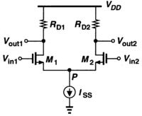
Fastest current switching will be achieved with unsaturated transistors. A differential pair as current switch and a continuously active (DC) current source connected to the common emitter/source node setting the current.
 

The glitch from the MOSFET at low currents may be due the large gate capacitance of a MOSFET. The path for the charge required to turn on the transistor goes through the source and drain junctions which then appears across the load.

A faster way to switch the current is to place the switch transistor directly across the load R1b. That way the constant-current circuit doesn't have to rapidly change it's current level, it will be essentially constant since the current either goes through the load or through the transistor. Of course this means the current will be constantly flowing, but I don't see that as a problem at these low current levels.

If the switch voltage is not equal to the supply voltage, then you will need to add an NPN transistor to drive the PNP across the load. This, of course, will invert the polarity of the switch control voltage (a high control voltage will then turn on the transistor and stop the current through the load).
 
Last edited:

    V

    Points: 2
    Helpful Answer Positive Rating
The load is r1b nd the circuit is working as controlled current sink
It will not act like a constant current sink. Nor will it act like a constant current source. This circuit is not a proper implementation of current control If you wanted to control current, you would feed back the bottom end of R1b to the op amp, because that is the voltage that best represents current. With the topology you now have, this circuit is more like a constant voltage regulator. The voltage at the emitter of Q1b is being controlled by the op amp to match the control voltage input. Unfortunately this feedback loop only works when there is some minimum current flowing through Q1b. When Q4 is off, this feedback control loop goes open loop. If you really do want to control current with the control voltage, you have to change this circuit quite a bit.
 

It will not act like a constant current sink. Nor will it act like a constant current source. This circuit is not a proper implementation of current control If you wanted to control current, you would feed back the bottom end of R1b to the op amp, ....................
Not true. The circuit shown is a common way to generate a constant current. The voltage across R7 is maintained constant by the op amp which means a constant current flows through R1b equal to the "control voltage" divided by the value of R7, independent an any variation with the value of R1b.

There is one error source in that circuit and that is the forward drop of transistor Q4 when it is on. That voltage will add a small error to the constant current value. This can be eliminated by connecting the (-) terminal of the op amp directly to the top side of R7, bypassing transistor Q4.
 
The circuit shown is a common way to generate a constant current.
Not so common and not so intelligent regarding the switching operation. In so far I agree with Tunelabguy. Although the OP output might stay in range, there's at least an unwanted transient injected into the constant current control loop.

A SPDT switch or at least a clamp circuit that allows the constant current to flow continuously would be preferred. I already mentioned the state-of-the-art method, which works up to GHz switching speed.
 

Feed back of the bottom end of R1b to the op-amp will not make a controlled current source/sink.
if we feedback the bottom end of R1b to the op amp then the current following through the load R1b will be (Vcc120-ControlVoltage)/R1b so the current will be dependent on the load .
This circuit is working fine as a voltage controlled constant current sink, It's already implemented and tested in the required range from 0 to 5mA with some simple modifications in resistor values
the idea is to apply a controlled voltage on a high precision resistor, and put the load in series with this resistor, then the current following through the load will equal the regulated voltage/the high precision resistor
 

the idea is to apply a controlled voltage on a high precision resistor, and put the load in series with this resistor, then the current following through the load will equal the regulated voltage/the high precision resistor
Yes that's o.k. so far, but adding the switching circuit creates problems that you reported.
 

Fastest current switching will be achieved with unsaturated transistors. A differential pair as current switch and a continuously active (DC) current source connected to the common emitter/source node setting the current.
May you give more info about this circuit or give reference to circuit diagram.
A SPDT switch or at least a clamp circuit that allows the constant current to flow continuously would be preferred. I already mentioned the state-of-the-art method, which works up to GHz switching speed.
and this too
 

Not true. The circuit shown is a common way to generate a constant current. The voltage across R7 is maintained constant by the op amp which means a constant current flows through R1b equal to the "control voltage" divided by the value of R7, independent an any variation with the value of R1b.

There is one error source in that circuit and that is the forward drop of transistor Q4 when it is on. That voltage will add a small error to the constant current value. This can be eliminated by connecting the (-) terminal of the op amp directly to the top side of R7, bypassing transistor Q4.
How does one maintain a constant current across a fixed resistor? Easy. Maintain a constant voltage across that resistor, in which case it is not a constant current source but a constant voltage source. A real constant current source holds the current constant despite changes in the resistance of the load. This circuit clearly does not do that. It is just a voltage regulator.
 

How does one maintain a constant current across a fixed resistor? Easy. Maintain a constant voltage across that resistor, in which case it is not a constant current source but a constant voltage source. A real constant current source holds the current constant despite changes in the resistance of the load. This circuit clearly does not do that. It is just a voltage regulator.
You seem be confusing the reference resistor with the load resistor. The circuit maintains a constant voltage across the reference resistor R7 which thus generates a constant current through R7. This same current flows through the load resistor R1b which is isolated from R7 by the Darlington stage U1b/Q1b and the op amp feedback. Thus a constant current flows through the load R1b independent of any variation in its resistance value (within the voltage limits of the supply of course).
 
You seem be confusing the reference resistor with the load resistor. The circuit maintains a constant voltage across the reference resistor R7 which thus generates a constant current through R7. This same current flows through the load resistor R1b which is isolated from R7 by the Darlington stage U1b/Q1b and the op amp feedback. Thus a constant current flows through the load R1b independent of any variation in its resistance value (within the voltage limits of the supply of course).
OK, I missed that the OP was considering R1b the load resistor.
 

May you give more info about this circuit or give reference to circuit diagram.
Consider a basic differential pair. Iss is the programmable current source, Vin is a switching signal, either differential or single ended feeding Vin1 only. Rd1 may be shorted, Rd2 is the load.


Status
Not open for further replies.

Similar threads

Part and Inventory Search

Welcome to EDABoard.com

Sponsor

Back
Top