RealAEL
Advanced Member level 1

- Joined
- May 16, 2008
- Messages
- 437
- Helped
- 298
- Reputation
- 598
- Reaction score
- 279
- Trophy points
- 1,343
- Location
- Hotel California
- Activity points
- 5,963
You are doing so many things WRONG here that I am not sure where to start.
Overall you do not seem to understand the difference between a linear and nonlinear model. The bias ALWAYS has to be applied to the nonlinear model directly. You cannot simulate a model without bias and then reuse that simulated data with the bias and expect it to work correctly. You should not be using the S2P symbol with the .ds data as the non-linear model. The .ds file is linear data because it was generated with an s-parameter simulation. Use the symbol original Avago model, ATF54143_dt.dsn, directly in the schematic.
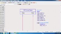
To evaluate the DC Bias of the device I would include this in a curve tracer schematic template ane simulate it there to determine the correct operating point.
The 31 Ohm resistor in the drain connection is totally wrong. I have never see and design built like that. Any change in current would change the drain voltage and alter the device performance. You should NEVER have resistors in series in that part of the amplifier. Why use a 5V DC source and simply throw away 2V in the resistor. Using a 3V DC source directly with no resistor should give a better Vdc operation.
A series 1600 pF capacitor in the input matching circuit does not seem right either. you would have many problems finding such a device that works correctly at 1.3GHz.
Before you start looking at the device in operation though you need to re-examine your design. Make sure that when you look at ONLY the input matching network with the bias network and ONLY the output matching network with the bias networks and do separate 2 port s-parameter simulations on each that you get the correct reflection coefficients (S22 for the input matching network and S11 for the output matching network) are as you requir for the design. Until that is correct the design will not work.

Schematic #1 af541433b_lineardevicemodel.dsn
1. The af541433b_dt_3_terminal.ds data is linear data at (at the wrong bias) so using this model is not correct.
2. You cannot do a DC simulation using a linear data model and get realistic answers.
3. The s-parameter simulation does not consider terminal voltages in the cirsuit so the DC source do not need to be there. They can be removed and replaced by grounds, they are effectively short circuit for s-parameter simulations or they could be annotated as "deactivated and shorted" or set to 0V. The important part is that the remainder of the biasing network should be included.
Schematic #2 54143_Original_EDABOARD_1.dsn
1. You cannot do a DC simulation using a linear data model and get realistic answers.
2. Same comments about the DC voltages source as in Schematic #1 above.
Schematic #3 af541433b_lineardevicemodel_withoutbias.dsn
1. The af541433b_dt_3_terminal.ds data is linear data at (at the wrong bias) so using this model is not correct.
Schematic #4 af541433b_dt_3_terminal.dsn
1. You are doing an s-parameter simulation of the circuit without the necessary bias. Reusing the model this way will never work. Take out the Term symbols and put back the original Ports (4 of them). Then use the symbol for this design file in the schematic for your design directly. This is the only way that this model should be used.
2. Even as is this device will not perform correctly as you have a disconnected wire for Term 3. You should never have red pin, red indicated a disconnected part.
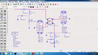
Your design should end up looking something like this for linear s-parameter simulation:

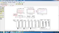
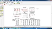
and for non-linear simulation:

Basically if you are using the af541433b_dt.dsn model downloaded from the Avago website and in any schematic that is used to simulate any circuit using that model if you do not see the same symbol for the packaged device then you are not doing it correctly.
Overall you do not seem to understand the difference between a linear and nonlinear model. The bias ALWAYS has to be applied to the nonlinear model directly. You cannot simulate a model without bias and then reuse that simulated data with the bias and expect it to work correctly. You should not be using the S2P symbol with the .ds data as the non-linear model. The .ds file is linear data because it was generated with an s-parameter simulation. Use the symbol original Avago model, ATF54143_dt.dsn, directly in the schematic.
To evaluate the DC Bias of the device I would include this in a curve tracer schematic template ane simulate it there to determine the correct operating point.
The 31 Ohm resistor in the drain connection is totally wrong. I have never see and design built like that. Any change in current would change the drain voltage and alter the device performance. You should NEVER have resistors in series in that part of the amplifier. Why use a 5V DC source and simply throw away 2V in the resistor. Using a 3V DC source directly with no resistor should give a better Vdc operation.
A series 1600 pF capacitor in the input matching circuit does not seem right either. you would have many problems finding such a device that works correctly at 1.3GHz.
Before you start looking at the device in operation though you need to re-examine your design. Make sure that when you look at ONLY the input matching network with the bias network and ONLY the output matching network with the bias networks and do separate 2 port s-parameter simulations on each that you get the correct reflection coefficients (S22 for the input matching network and S11 for the output matching network) are as you requir for the design. Until that is correct the design will not work.
Schematic #1 af541433b_lineardevicemodel.dsn
1. The af541433b_dt_3_terminal.ds data is linear data at (at the wrong bias) so using this model is not correct.
2. You cannot do a DC simulation using a linear data model and get realistic answers.
3. The s-parameter simulation does not consider terminal voltages in the cirsuit so the DC source do not need to be there. They can be removed and replaced by grounds, they are effectively short circuit for s-parameter simulations or they could be annotated as "deactivated and shorted" or set to 0V. The important part is that the remainder of the biasing network should be included.
Schematic #2 54143_Original_EDABOARD_1.dsn
1. You cannot do a DC simulation using a linear data model and get realistic answers.
2. Same comments about the DC voltages source as in Schematic #1 above.
Schematic #3 af541433b_lineardevicemodel_withoutbias.dsn
1. The af541433b_dt_3_terminal.ds data is linear data at (at the wrong bias) so using this model is not correct.
Schematic #4 af541433b_dt_3_terminal.dsn
1. You are doing an s-parameter simulation of the circuit without the necessary bias. Reusing the model this way will never work. Take out the Term symbols and put back the original Ports (4 of them). Then use the symbol for this design file in the schematic for your design directly. This is the only way that this model should be used.
2. Even as is this device will not perform correctly as you have a disconnected wire for Term 3. You should never have red pin, red indicated a disconnected part.
Your design should end up looking something like this for linear s-parameter simulation:
and for non-linear simulation:

Basically if you are using the af541433b_dt.dsn model downloaded from the Avago website and in any schematic that is used to simulate any circuit using that model if you do not see the same symbol for the packaged device then you are not doing it correctly.
Last edited:

