moin.gadiwan27
Newbie level 2

Hi,
This is Moin here.
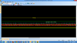
I have a schematics which is 1173.0mm length and width 18mm (tube light).
In PADS I have designed layout.
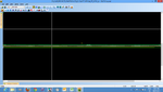
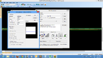
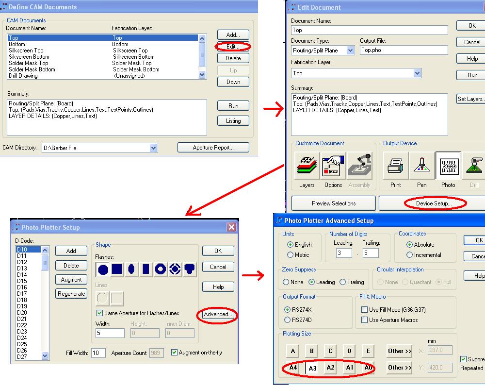
But generating Gerber is not possible as shown in the diagram 1,2,3.
Please help me in solving these issue.
This is Moin here.
I have a schematics which is 1173.0mm length and width 18mm (tube light).
In PADS I have designed layout.
But generating Gerber is not possible as shown in the diagram 1,2,3.
Please help me in solving these issue.