Continue to Site

Welcome to EDAboard.com

Welcome to our site! EDAboard.com is an international Electronics Discussion Forum focused on EDA software, circuits, schematics, books, theory, papers, asic, pld, 8051, DSP, Network, RF, Analog Design, PCB, Service Manuals... and a whole lot more! To participate you need to register. Registration is free. Click here to register now.

LDO Design Problem. Pmos pass transistor going subthreshold region

Status
Not open for further replies.

kishore680

Member level 5
Member level 5
Joined
Mar 14, 2012
Messages
81
Helped
3
Reputation
6
Reaction score
4
Trophy points
1,298
Location
Bangalore
Activity points
1,833
I have done LDO design. Input voltage is 2-2.4 V
Output voltage=1.8v.
maximum load current=50mA
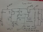
2013-06-26 20.26.11.jpg

I m getting this output voltage but Pmos pass transistor is going to sub threshold region. Vref=1.16v.
what should be the output of differential pair(Single ended output).what should be done to operate it on saturation region

p.s: I had earlier done 2 stage opamp. TAking output at CS stage. But still no use. why is so?
Please help me designing it
 
Have you considered designing the pass transistor with a Vds sat of 150mV? and then setting W & L for 50mA?

Subthreshold is when the overvoltage Vov is between 70mV to 100mV, so for strong inversion you will need ~ 150mV vov which is the same as Vds sat. Does this help?
 

should i change W/L of PMOS Pass transistor. Since i ve kept 6m/180n. how about changing voltage at differential pair output?. Since controlling action is done. It will always change . But its voltage should be always less such that Vgs>Vt. Vt=0.4928v. How to achieve
 

Your active load vd sat will probably be around 0.3 v for the diode connected transistor you could redesign the diff input but i think better to do pass transistor.

Substitute 100mv into vgs minus vt then rearrange to find a new width. As vds sat decreases width mst incrase for a set constant current . Does this help explain.
 

maximum load current=50mA

I m getting this output voltage but Pmos pass transistor is going to sub threshold region. Vref=1.16v.
... what should be done to operate it on saturation region

Hello kishore,

subthreshold is not an operating region (meaning a region in the output characteristic of a transistor), it is a mode of operation. If your load current IL«IL,max, it is quite normal that your pass transistor works in subthreshold mode (|Vgs| < |Vth|) - this is totally ok. Don't get confused by the Cādence' message subthreshold - it just means that your W/L ratio might be too large for the used current - but it will still work in saturation region (|Vds| > |Vds,sat|). Keep your large W/L - you'll need it for your max. load current, then the pass transistor probably will work in the triode region - in saturation region only for small and medium load currents.

erikl
 
Hi Kishore,

I totally go with erikl version & as mentioned, if the load current where it goes to subthreshold is too less compared to max load. And even @ low load current if you still want the pass transistor to be strong inversion, then most probably you reduce the device dimensions a lot & which pushes the previous region to linear (5 pack being the first stage) @ max load currents. Rather the better option is to allow them in sub threshold. And in general the offsets are not a concern at all in LDO rather the most important is the load regualtion.
 
Oh thanks for clarifying. I think i should check vds of the pass transistor and vdsat.I think it will satisfy the condition Vds>vdsat(Because i'm getting output voltage as 1.8v).. And yeah i kept W/L very high only considering Ilmax=50 mA. So for all other loads Il<Ilmax.So it shows subthreshold i.e Region=3 in cadence
 
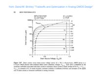
Just to clarify the necessity for your pass transistor to work in medium (M.I.) and in weak inversion (W.I.), i.e. subthreshold mode: see this figure from Binkley's book: .

Even if it stems from an NMOSFET with W/L=16 you can approximately transfer it to your PMOS, multiplying the log. y-axis by a factor of 1000, i.e. mA instead of µA. For your min. input-output voltage difference |Vds,min| of |0.2V| - and still achieving a good regulation - you should try and work with a |VDS,sat| <≈ |Vds,min|, i.e. with an Inversion Coefficient IC ≦ 5 , which means M.I. mode for your 50mA output current. Subthreshold operation (|Vgs| ≦ |Vth|) starts at IC <≈ 0.5, hence with an output current ≦ 5mA your pass PMOSFET will work in subthreshold mode, below 1mA in W.I. mode (IC ≦ 0.1) - and this is totally ok, because only then you can have such low VDS,sat and so can guarantee to still work in the saturation region |VDS,sat|≦|Vds| where you have much better regulation (gain) than in the triode (or linear) region |Vds|≦|VDS,sat|.
 
Hi Erikl,

Thank you for the reference and detailed feedback regarding this question. Very helpful!
 

Hey erikl i have designed the LDO for those conditions.LDO pass element has W/L=9m/1u. what about stability of this LDO. what all need to be considered. Does that capacitor with ESR will make sure about stability all the time? By nullifying one pole?
 

Hi kishore, LDO design is a wide theme, and I think this is not the right place to educate you - nor do I have the time to do so, sorry. There are a lot of papers available on all these subjects, study them! Run your simulations, stability and others, and come back with concrete questions, if you need help.
 

Attachments

  • A_Linear_LDO_Regulator_with_Modified_Frequency_Compensation_Independent_of_Off-chip_Capacitor_an.pdf
    499.7 KB · Views: 226
  • cap_less_LDO_chargePump.pdf
    513.5 KB · Views: 242
  • ESR_and_Stability_of_LDO_Regulator.pdf
    76.9 KB · Views: 223
  • Operation_and_Compensation_of_LDOs_NS-AN-1148.pdf
    199.6 KB · Views: 200
  • Stability_in_High_Speed_Linear_LDO_Regulators_ON_AND8037-D.pdf
    164.5 KB · Views: 160
  • stable_ESR_range_of_LDO.pdf
    148.8 KB · Views: 331
  • Weblocs.zip
    10 KB · Views: 157
ya thanks i went through some.But how to perform ac analysis of LDO. I mean Bode plot.To find gain and phase margin. In CADENCE . IT would be very helpful if i get to knw the procedure.
 

Attachments

  • CADENCE_Design_Environment_Tutorial.pdf
    1.6 MB · Views: 222
  • Cadence_Flow_(Virtuoso)_for_a_CMOS_Inverter_Design.pdf
    2 MB · Views: 202
  • CADENCE_intro_front_to_back.pdf
    1.9 MB · Views: 228

Status
Not open for further replies.

Similar threads

Part and Inventory Search

Welcome to EDABoard.com

Sponsor

Back
Top