Nick_F
Member level 1

Hi All,
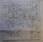
The image I attach is from a 40V power supply that was published by (now defunct) Electronics Australia and it was sold by Dick Smith Electronics in Australia as kit K-3206 (Versatile 40V/3A Lab Power Supply).
It is voltage adjustable 0 to 40V and also has adjustable current limiting 0 to 3A, has over-temperature protection and ripple warning. Also, it is a dual tracking power supply.
I built the power supply some years ago, and it appeared to work fine, when doing measurements with a voltmeter. At that time, I didn't have an oscilloscope.
The PCB is home made and it is not something I can be proud of. I followed the original layout design.
What I found after using it: When turning the power supply ON/OFF, there is a large spike of voltage, with an amplitude up to 30V or so. It appears especially about 1 second after turning the power off. If the power supply is set on 5V and supplies a PIC microcontroller, when turning it off it will almost always blow the microcontroller.
Another issue is that the output has a tendency to autooscillate even for purely resistive loads. When using an oscilloscope on the outputs under load, I can see oscillation of a few MHz, especially when connecting the load between + and - (no common zero used).
In order to identify the area that generates oscillations, I connected anode of D1 (point A) at +12V, effectively disabling the current limiting function. It appears to me that IC1a+Q1+Q2 oscillates, as well as IC2a+Q3+Q4.
I also added some hundreds of pF capacitors between the inverting input and the output of IC1a, IC2a, but all I can obtain is sometimes changing the amplitude and frequency of the oscillation. I also tried various values for C4. I concentrated on the positive rail power supply (built around IC1 and Q1), which oscillates when it has a resistive load between 0 and +OUT.
One problem I solved was that IC6 was also oscillating, because the designers didn't bother to put some capacitors from the outputs to ground for the 7812, 7912 regulators.
I would build another PCB for this power supply, provided the circuit diagram has capability to work properly. Ideally, I would like to tame the oscillations on the present PCB.
I hope somebody with more experience than me would advise if this diagram is worth building.

Regards,
Nicolae
The image I attach is from a 40V power supply that was published by (now defunct) Electronics Australia and it was sold by Dick Smith Electronics in Australia as kit K-3206 (Versatile 40V/3A Lab Power Supply).
It is voltage adjustable 0 to 40V and also has adjustable current limiting 0 to 3A, has over-temperature protection and ripple warning. Also, it is a dual tracking power supply.
I built the power supply some years ago, and it appeared to work fine, when doing measurements with a voltmeter. At that time, I didn't have an oscilloscope.
The PCB is home made and it is not something I can be proud of. I followed the original layout design.
What I found after using it: When turning the power supply ON/OFF, there is a large spike of voltage, with an amplitude up to 30V or so. It appears especially about 1 second after turning the power off. If the power supply is set on 5V and supplies a PIC microcontroller, when turning it off it will almost always blow the microcontroller.
Another issue is that the output has a tendency to autooscillate even for purely resistive loads. When using an oscilloscope on the outputs under load, I can see oscillation of a few MHz, especially when connecting the load between + and - (no common zero used).
In order to identify the area that generates oscillations, I connected anode of D1 (point A) at +12V, effectively disabling the current limiting function. It appears to me that IC1a+Q1+Q2 oscillates, as well as IC2a+Q3+Q4.
I also added some hundreds of pF capacitors between the inverting input and the output of IC1a, IC2a, but all I can obtain is sometimes changing the amplitude and frequency of the oscillation. I also tried various values for C4. I concentrated on the positive rail power supply (built around IC1 and Q1), which oscillates when it has a resistive load between 0 and +OUT.
One problem I solved was that IC6 was also oscillating, because the designers didn't bother to put some capacitors from the outputs to ground for the 7812, 7912 regulators.
I would build another PCB for this power supply, provided the circuit diagram has capability to work properly. Ideally, I would like to tame the oscillations on the present PCB.
I hope somebody with more experience than me would advise if this diagram is worth building.

Regards,
Nicolae
