Terminator3
Advanced Member level 3

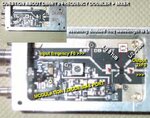
Hello! I found nice design of frequency doubler here: http://members.datafast.net.au/vk3zqb/24proj.htm

Frequency F0 going from left to right until doubled. From left to right:
1. "?" widened microstrip area
2. modulation DC bias
3. L/4 stub for filtering 2xF0 frequency out (L is wavelength of 2xF0)
4. antiparallel diode pair for mixing/doubling purpose
5. L/2 stub for filtering F0 (acts as L/4 stub for F0)
6. again some "?" widened microstrip area.
So what the purpose of two widened microstrip areas? I guess it is not quarterwave matching line.
It looks that it is quarter-wavelength (for 2F0 before diodes and for F0 after diodes).
If it is some kind of unwanted freq reflection method, what impedance of this lines i must choose?
Thanks!
