Continue to Site

Welcome to EDAboard.com

Welcome to our site! EDAboard.com is an international Electronics Discussion Forum focused on EDA software, circuits, schematics, books, theory, papers, asic, pld, 8051, DSP, Network, RF, Analog Design, PCB, Service Manuals... and a whole lot more! To participate you need to register. Registration is free. Click here to register now.

Common centroid cross coupled for six MOS transistors

Status
Not open for further replies.

Junus2012

Advanced Member level 5
Joined
Jan 9, 2012
Messages
1,552
Helped
47
Reputation
98
Reaction score
53
Trophy points
1,328
Location
Italy
Activity points
15,235
Hello friends

I have 6 transistors (A,B,C,D,E,F) represent the parts of the current mirror in the current mirror amplifier.

D,E,F are five times larger than A,B,C in order to get the factor K=5.

could you please suggest me the array of this mirror in common centroied cross-coupled.

Thank you
 

is it possible to make A,B,C with m=3 and D,E,F with m= 15 ???
 

Hello Senan,

absolute common centroid isn't possible with a minimum array. But perhaps you like this one?

Code:
DEFY
FADE
FEDC
DBFE
DEFY

Y are dummies.
 
thank you erikl :):)
you always helping me with my layout issue

from your array you mean to say I have to repeat it three times to get my desired ratios.

one more thing, I am thinking that the layout of my OTA becoming a little complicated, do you think so or it is common to have like this?
thank you again
 

from your array you mean to say I have to repeat it three times to get my desired ratios.
No: In the above array you already have 1 MOS A, B & C, and 3 each from D, E & F (=18 + 2 dummies). So one array is enough.

one more thing, I am thinking that the layout of my OTA becoming a little complicated, do you think so or it is common to have like this?
I think it's enough to have a good matching between the input transistors, a very good matching (large W/L, common centroid -- as good as possible -- dummies around to keep the physical environment), if you need small offset voltage. For the mirror transistors, common centroid is not so important, I think, as their matching accuracy is not important for the OTA function. Just keep them close together, and if possible interdigitize the fingers of 2 equal transistors to be paired (load and cascode transistors).

Perhaps you should try and find layouts from other OTAs to study how they are designed. Searching for "OTA layout" in G00GLE images will show you 2 of those in the first row, one of them even including the schematic topology.
 
thank you erikl
you are right regarding the importance of the input transistors and the mirror transistors. but for me the accuracy of the mirror is never the less is also important as my OTA is current mirror topology.

for the array arrangement, I am restricted in my design to use A,B,C with m=3 and this is why I asked you that I must repeat your suggested array three times. is that possible ?
Thank you in advance
 

for the array arrangement, I am restricted in my design to use A,B,C with m=3 and this is why I asked you that I must repeat your suggested array three times. is that possible ?

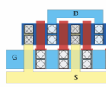
I'd suggest to use (for all of them) one transistor with 3 fingers (f=3). So you can get along with a single array.
 

HI,

I suggest that use Inter digitization matching pattern keeping DIODE device at the center for the current mirrors.

Inform me the diode device details and name .

regards,
Basu

- - - Updated - - -

I'd suggest to use (for all of them) one transistor with 3 fingers (f=3). So you can get along with a single array.

If we make one transistor =3 fingers then it is difficult to share the diffusion or you can say connection with other devices. Otherwise you need to break up the diffussion which increases the parasitic and not a good idea for matching in lower tech nodes.
I would say always make one transistor = Even fingers.

Regards,
Basu
 
Last edited:
f=3 to m=3 comparison

I would say always make one transistor = Even fingers.

You are totally right, bgangur, but he (Junus, or Senan) told to be restricted to m=3 (for a single multiple transistor, he didn't tell why). So I suggested to use f=3 instead, which will certainly decrease the parasitic capacitance in comparison to an m=3 construction.

3-finger-MOSFET.png
 
Status
Not open for further replies.

Part and Inventory Search

Welcome to EDABoard.com

Sponsor

Back
Top