Continue to Site

Welcome to EDAboard.com

Welcome to our site! EDAboard.com is an international Electronics Discussion Forum focused on EDA software, circuits, schematics, books, theory, papers, asic, pld, 8051, DSP, Network, RF, Analog Design, PCB, Service Manuals... and a whole lot more! To participate you need to register. Registration is free. Click here to register now.

Gate oxide breakdown issue with extracted simulations

Status
Not open for further replies.

viperpaki007

Full Member level 5
Full Member level 5
Joined
Jul 2, 2008
Messages
274
Helped
11
Reputation
22
Reaction score
8
Trophy points
1,298
Location
Finland
Activity points
3,437
Hi I am making a clock distribution circuit working at 4GHz. Generated clock is needed by flipflops. I tried to route the clock in such way that the distance of clock source to all flipflops remain same. Moreover, i put a ground line between clock signals to reduce interference. However, as soon as i do the extracted simulations with interconnect parasitics, i observe the following warning msg from spectre and the simulations do not proceed further.

Vgs has exceeded the oxide breakdown voltage of `vbox'=2.6V

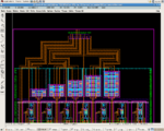
My supply voltage is 1.2V and the circuit works properly without the parasitic extraction. Therefore, i assume that there is some problem with layout design which is causing some interference glitch to appear at the transistors and increase the voltage beyond the gate oxide breakdown voltage. I am attaching the screenshots of my layout. Can somebody suggest what should i do to avoid this problem.

I have already tried to add a capacitor between vdd and vss lines but it does not solve the problem Screenshot.png
 

Hi,

What kind of extraction ? RLC or RC only ?
Is it a regular or "rf" simulation ?
 

I am extracting R+C+CC+L+M so in short it is RLC with mutal inductance and capacitances
 

Plot Vgs to find out where you get the overvoltage. I'd suppose the parasitic L is the culprit (check by removing it/them). Try to compensate by additional capacitance in parallel to Vgs .
 
Additional capacitance will clearly "kill" the overshoot, but there is probably a more elegant solution.
For example try a smaller rise time
 
Additional capacitance will clearly "kill" the overshoot, but there is probably a more elegant solution.
For example try a smaller rise time

I think both methods aren't easily to be adjusted for a 4GHz clock network.
 
I see a lot of this, coming from charge pumping and unrealistic
leakage ("off") models, in switching circuits where there is a
break-before-make action.

Your BVox number asserted in the PDK, is probably a reliability
long-term number and a subnanosecond spike can be withstood
most likely. I would capture one such event (drill down to the
offendor and plot terminals) and then get a reading from your
foundry reliability people on the short-pulse oxide withstand
voltage, along with doing some sanity checking of the voltages
you're seeing.

You may also want to play some, with tolerances and numerical
methods to assure youself about the realism of the result.
 

What is the length of your clock lines? Will it pass the antenna check?
You could add small driver buffer into 1 line just to see it the issue goes away. I would think that paratitic inductance could be the culprit.
Or you can look into the PEX values and add little LC tank into schematic and re-run the schematic sim.(probably easier)
 
Status
Not open for further replies.

Part and Inventory Search

Welcome to EDABoard.com

Sponsor

Back
Top