Continue to Site

Welcome to EDAboard.com

Welcome to our site! EDAboard.com is an international Electronics Discussion Forum focused on EDA software, circuits, schematics, books, theory, papers, asic, pld, 8051, DSP, Network, RF, Analog Design, PCB, Service Manuals... and a whole lot more! To participate you need to register. Registration is free. Click here to register now.

[SOLVED] Can someone check if this PCB Layout and guide me further?

Status
Not open for further replies.

pcsandhya82

Member level 3
Member level 3
Joined
Jul 31, 2010
Messages
58
Helped
0
Reputation
0
Reaction score
0
Trophy points
1,286
Location
Bangalore
Activity points
1,732
Hello,

I am experimenting with eagle.

Can someone please look at this small project I have done in eagle? Its a temperature control using PIC16F877. I have taken a construction from EFY, they have given the PCB Layout. I have tried to reproduce that.

I have attached the project. Please tell me if there are any errors.

Also, I am not able to get those GND and VCC planes to cover the available area on the board. How do I do that?
 

Attachments

  • PIC16F_LM35.rar
    479.4 KB · Views: 157
  • pic.rar
    34.2 KB · Views: 160

Hi,
You can check for any errors using Eagle; In schematic view, Go to Tool menu and select ERC. That will give list of errors and warnings. Check them; all of them may not be corrected if you aware that they are not useful for the function of circuit. Also in Board view select Errors in tools menu.
(there is one obvious error in Board view; one route passes across several pins of LCD, must be corrected )
Thanks,


For generating Ground plane see following instructions;
https://tangentsoft.net/elec/movies/tt10.html
 
Last edited:
Hi,

Thanks a lot for all the help..

I have made some changes. Can some one suggest a good tutorial to understand DRC parameters better? Also, is there any errors in what I have done? How can I get it fabricated in India?

I have attached the schematics and board, and their pictures.
 

Attachments

  • PIC16F_LM35.rar
    88.9 KB · Views: 141

It seems to be ok with your modifications. Design rule check is a facility that you can adjust PCB design parameters; most of them are illustrated in each tab of DRC.
I hope some one will help you to find PCB fabrication service in Bangalore.

For that size of PCB you can make it your self !
You will need a Glossy paper (or press n' peel paper) and etching chemical (Ferric chloride or HCl and Hydrogen peroxide)
pcbpapn.jpg
Search the youtube for "PCB with toner transfer method"
https://www.youtube.com/watch?v=bk6WJpGyc4I
 

On the shematic I recommend you bigger R2 resistor...at least 10K to minimize current drain on reset pin..on the most shematics it is 10K..but it will work.
Electrolyte capacitor on output of LM7805 is recommended to compensate current peaks from loads (uC, display etc), also caramic 330pF on input is recomanded.
About PCB: Learn to save place, that knowledge will be important in future bigger prijects. For example, oscillator and capacitors (22p) can be placed below uC, move a little bit LED and you already save 1cm of plate. Put your regulator that metal side is directed outside board...so if you need heatsink it is easier to put it. Don't hesitate to use vias if that can save your plate...even if you make one layer board you can use wires to connect lines in top layer.
Remember, cheap and small design is well appriciate in electronics.
 

Hi,

I edited the layout to save some more space. Then ran DRC and there are no errors. I processed the CAM job with sparkfun's sfe-gerb274x.cam file. and i check the gerber in http://www.viewplot.com/ gerber viewer and it flashes there are 14 errors, but do not list out any errors. I m attaching the project here, can some one please look into it?
 

Attachments

  • PIC16F_LM35-v1.rar
    84.7 KB · Views: 159

The most likely errors are silk screen on the pads. Some manufacturers will clip the silk screen for you, otherwise you have to do it yourself. Turn on all layers in Eagle and do the DRC and you will see the errors (although there are a lot more than 14 so I guess viewplot only cares about some of them).

Keith
 
You have large areas of copper that do not actually do anything except act as antennas. These large areas neck down to narrow (high impedance) traces through the device pins. Remove these areas and just use a thick track, you EMI immunity will be much better.

Some info on planar antennas, dont worry about the text so much look at pictures, so you can relate these to the areas of copper you have on your design. The big problem with these sort of copper structures is that they are good at picking up braodband RF not what you realy want.
http://hibp.ecse.rpi.edu/~connor/education/Antennas/NSYSU2.pdf
**broken link removed**
http://scholar.lib.vt.edu/theses/available/etd-08262002-183120/unrestricted/PHD_DISSERTATION_SUH.pdf
 
Hi,

@marce , I had reproduced a board which has lots of these copper area. Have attached it with this. will go through the papers that you posted.

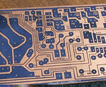
I have sent the board for fabrication, and i m attaching the image of the PCB that the fabhouse sent me here. it looks fine to me. Could anyone go through it?
 

Attachments

  • 184666-PCB_image.pdf
    129.4 KB · Views: 163
  • pic.bmp
    1 MB · Views: 152

Can someone check if this PCB image from the fab house is error free?

Hi,
This is my first design going to the fab house and they sent me back this picture. I see the silk screen is marked in the bottom layer. is this a mistake?

Are there any other mistakes? I have attached the complete design in this thread:
https://www.edaboard.com/threads/264411/

attaching the image from the fab house here.
 

Attachments

  • 184666-PCB_image.pdf
    129.4 KB · Views: 171

Re: Can someone check if this PCB image from the fab house is error free?

hi,
ya mistake only.. you should mention the silkscreen in TOP because your component has mounded in top side so you should assign in top only if your component mound in bottom you can assign the silkscreen in bottom.

which tool r u using now it's appearance is to good ???
 

Re: Can someone check if this PCB image from the fab house is error free?

well the fabhouse haven't marked any error.t PCB is OK , you should have used thicker traces to connect the ground planes copper. you mentioned there is no DRC errors,and these pictures from fabhouse also don't show any errors
 

Re: Can someone check if this PCB image from the fab house is error free?

hi sherazi,

in PDF Bottom view silkscreen should not come right ?? we have assign the separate layer for silkscreen
 

Re: Can someone check if this PCB image from the fab house is error free?

i checked your PCB file and it has the silk on top . the fabhouse is referring to top layer as bottom layer and to bottom as top
nothing to worry about
 
Status
Not open for further replies.

Part and Inventory Search

Welcome to EDABoard.com

Sponsor

Back
Top