Continue to Site

Welcome to EDAboard.com

Welcome to our site! EDAboard.com is an international Electronics Discussion Forum focused on EDA software, circuits, schematics, books, theory, papers, asic, pld, 8051, DSP, Network, RF, Analog Design, PCB, Service Manuals... and a whole lot more! To participate you need to register. Registration is free. Click here to register now.

[SOLVED] PIC Delay Subroutine not working (PIC16F886)

Status
Not open for further replies.

qbone

Member level 3
Member level 3
Joined
Jun 2, 2009
Messages
58
Helped
0
Reputation
0
Reaction score
0
Trophy points
1,286
Location
Lyngby, Denmark
Activity points
1,778
Hey guys.

I am currently trying to learn assembly programming of PIC processors, and is following the tutorial on pcbheaven.com.
I have reached the point where I need to get an LED to flash, but it just wont :(

The tutorials are aimed for a PIC16F88, but I am converting it to fit my PIC as I go on, and I THINK I have done it right so far - but I guess its not all right since it doesnt work :oops:

I have searched high and low and found an answer on this forum where someone tells a guy to use the delay routine generator located at
I have tried that and implemented my code, but it still doesnt work.

Here are my code:
Code:
 list       F=inhx8m, P=16F886, R=hex, N=0
#include <P16F886.INC> ; PIC definitions
 __config _config1,_INTOSCIO & _WDT_OFF & _LVP_OFF & _PWRTE_OFF & _MCLRE_OFF & _BOREN_ON & _LVP_OFF & _CPD_OFF & _WRT_OFF & _CP_OFF
 __config _config2,_IESO_OFF & _FCMEN_OFF  
 Errorlevel -302      ; switches off Message [302]: Register in operand not in bank 0.

; RAM preserved -----------------------------------------------------------
	cblock 0x20
		WaitCounter,WaitCounter2
	endc
; Program Memory ----------------------------------------------------------
                org     0
                goto    Init
; Interrupt Service Routine -----------------------------------------------
                org     4               ; ISR beginning
; Microcontroller initialization
Init            
			include init_normal.inc	;Include the PIC Initialization routine
; Main Program ------------------------------------------------------------
Start
			bank1

			movlw b'11111111'	;Set the port pin types of the RA
			movwf TRISA			;All RA ports are inputs

			movlw b'11111110'	;Set the port pin types of the RB
			movwf TRISB			;All RB ports are input except RB0 that is output

			bank0				;Go to bank 0
MainLoop
			bsf PORTB,0			;Set RB0 output LOW
			call Delay
			bcf PORTB,0			;Set RB0 output HIGH
			call Delay
			goto MainLoop		;And go back to the Main Loop

			; Delay = 0.5 seconds
			; Clock frequency = 4 MHz
			
			; Actual delay = 0.5 seconds = 500000 cycles
			; Error = 0 %
			
				cblock
					d1
					d2
					d3
				endc
			
			Delay
						;499994 cycles
				movlw	0x03
				movwf	d1
				movlw	0x18
				movwf	d2
				movlw	0x02
				movwf	d3
			Delay_0
				decfsz	d1, f
				goto	$+2
				decfsz	d2, f
				goto	$+2
				decfsz	d3, f
				goto	Delay_0
			
						;2 cycles
				goto	$+1
			
						;4 cycles (including call)
				return
Fins            
                end             ; end of program

And before someone asks, this is the content of init_normal.inc :

Code:
				bank1
				movlw b'01100000'
				movwf OSCCON
WaitForStableOscillator
				btfss OSCCON,HTS
				goto WaitForStableOscillator

                movlw b'11111000'		; OPTION_REG setup
                movwf option_reg             
                clrf pie1				;
                clrf pie2				; No peripherial interrupt
                clrf txsta				;Disable AUSART
				;PSA must be to WDA (bsf OPTION_REG,psa)
				bcf OPTION_REG,PS2
				bcf OPTION_REG,PS1
				bsf OPTION_REG,PS0
				clrf adcon1				;No analog to digital conversion
				bank3
                clrf ansel				; No analog to digital conversion
                clrf anselh				; No analog to digital conversion
				bank2
				clrf CM1CON0		;disable Comparator
				clrf CM2CON0		;disable Comparator
				clrf CM2CON1		;disable Comparator
				bank0
				;General
                clrf rcsta				;Disable AUSART receive
				clrf adcon0				;No analog to digital conversion

I am programming in MPAB v8.85 and my programmer is a Olimex PIC-MCP-USB (Basicly a PICSTART+, atleast thats what they say :p)

- - - Updated - - -

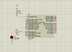
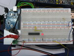
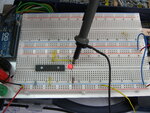
This is my setup on the breadboard http://pcbheaven.com/picpages/images/ledflasher_1250600962.jpg (again - I am using PIC16F886, so I just did the same more or less.)
 

Hi,

Yes you are very close to getting it running, though as you will see from your Build you do get errors.

Below is your code silghtly modified as follows

The BANK1 instructions are invalid, you must use the banksel directive, as shown, eg banksel TRISA to enter bank1, once in bank1 you do not have to use banksel again until you move to another bank
To get back to bank 0 you can use banksel 0, you cannot use banksel 1 etc.

Also you have specified your Delay routine registers d1,d2,d3 but not specified any location have placed them up with you main cblock 0x20.

You should find these tutorials helpful.
http://www.winpicprog.co.uk/pic_tutorial.htm
( though his adc hardware is overkill, for a simple demo just use a 10k trimmer direct to the adc pin
**broken link removed**

Code:
	 list       F=inhx8m, P=16F886, R=hex, N=0
	#include <P16F886.INC> ; PIC definitions
	 __config _config1,_INTOSCIO & _WDT_OFF & _LVP_OFF & _PWRTE_OFF & _MCLRE_OFF & _BOREN_ON & _LVP_OFF & _CPD_OFF & _WRT_OFF & _CP_OFF
	 __config _config2,_IESO_OFF & _FCMEN_OFF  
	 Errorlevel -302      ; switches off Message [302]: Register in operand not in bank 0.

; RAM preserved -----------------------------------------------------------
	cblock 0x20
		WaitCounter,WaitCounter2
		d1,d2,d3
	endc
; Program Memory ----------------------------------------------------------
                org     0
                goto    Init
; Interrupt Service Routine -----------------------------------------------
                org     4               ; ISR beginning
; Microcontroller initialization
Init            
;			include init_normal.inc	;Include the PIC Initialization routine

				banksel OSCCON
				movlw b'01100000'
				movwf OSCCON
WaitForStableOscillator
				btfss OSCCON,HTS
				goto WaitForStableOscillator

                movlw b'11111000'		; OPTION_REG setup
                movwf option_reg             
                clrf pie1				;
                clrf pie2				; No peripherial interrupt
                clrf txsta				;Disable AUSART
				;PSA must be to WDA (bsf OPTION_REG,psa)
				bcf OPTION_REG,PS2
				bcf OPTION_REG,PS1
				bsf OPTION_REG,PS0
				clrf adcon1				;No analog to digital conversion
				bankSEL ANSEL
                clrf ansel				; No analog to digital conversion
                clrf anselh				; No analog to digital conversion
				bankSEL CM1CON0
				clrf CM1CON0		;disable Comparator
				clrf CM2CON0		;disable Comparator
				clrf CM2CON1		;disable Comparator
				banksel 0
				;General
                clrf rcsta				;Disable AUSART receive
				clrf adcon0				;No analog to digital conversion

;I am
; Main Program ------------------------------------------------------------
Start
			banksel TRISA

			movlw b'11111111'	;Set the port pin types of the RA
			movwf TRISA			;All RA ports are inputs

			movlw b'11111110'	;Set the port pin types of the RB
			movwf TRISB			;All RB ports are input except RB0 that is output

			banksel 0				;Go to bank 0
MainLoop
			bsf PORTB,0			;Set RB0 output LOW
			call Delay
			bcf PORTB,0			;Set RB0 output HIGH
			call Delay
			goto MainLoop		;And go back to the Main Loop

			; Delay = 0.5 seconds
			; Clock frequency = 4 MHz
			
			; Actual delay = 0.5 seconds = 500000 cycles
			; Error = 0 %
			
	
Delay
						;499994 cycles
				movlw	0x03
				movwf	d1
				movlw	0x18
				movwf	d2
				movlw	0x02
				movwf	d3
Delay_0
				decfsz	d1, f
				goto	$+2
				decfsz	d2, f
				goto	$+2
				decfsz	d3, f
				goto	Delay_0
			
						;2 cycles
				goto	$+1
			
						;4 cycles (including call)
				return
Fins            
                end             ; end of program
**broken link removed**
 

Attachments

  • ScreenShot001.jpg
    ScreenShot001.jpg
    55.6 KB · Views: 126
  • Like
Reactions: qbone

    qbone

    Points: 2
    Helpful Answer Positive Rating
Hi wp100, thanks alot for taking a look.
The first things your are adressing concering the BANK selection, that is completely my bad.
I forgot to include that I in PIC16F886 have included the following code:

Code:
; Definitions of Bits
#define carry   status,c ; STATUS register
#define dcarry  status,dc
#define zero    status,z


; Macros
Bank0   macro
        bcf     status,rp1
        bcf     status,rp0        ; BANK0 (Data Memory)
        ;bcf     status,irp
        endm

Bank1   macro
        bcf     status,rp1
        bsf     status,rp0        ; BANK1 (Data Memory)
        ;bcf     status,irp
        endm

Bank2   macro
        bsf     status,rp1
        bcf     status,rp0        ; BANK2 (Data Memory)
        ;bsf     status,irp
        endm

Bank3   macro
        bsf     status,rp1
        bsf     status,rp0        ; BANK3 (Data Memory)
        ;bsf     status,irp
        endm

But after that, you are completely right, I forgot to specify where I wanted the d1,d2,d3 registers stored, but that didn't fix my problem :( When I run in it MPLAB SIM it looks like it is getting stuck in some endless loop when counting down d1.

I read on a little further in the tutorials and found a routine he is using, and I modified it very slightly so I could paste it into my code, and this is what I got so far:

Code:
; RAM preserved -----------------------------------------------------------
			cblock 0x20
				WaitCounter,WaitCounter2
			endc
; Program Memory ----------------------------------------------------------
                	org     0
                	goto    Init
; Interrupt Service Routine -----------------------------------------------
                	org     4               ; ISR beginning
; Microcontroller initialization
Init            
			include init_normal.inc	;Include the PIC Initialization routine
; Main Program ------------------------------------------------------------
Start
			bank1

			movlw b'11111111'	;Set the port pin types of the RA
			movwf TRISA		;All RA ports are inputs

			movlw b'11111110'	;Set the port pin types of the RB
			movwf TRISB		;All RB ports are input except RB0 that is output

			bank0				;Go to bank 0

MainLoop
			bsf PORTB,0		;Set RB0 output LOW
            		call Wait1mSec
			bcf PORTB,0		;Set RB0 output HIGH
            		call Wait1mSec
			goto MainLoop		;And go back to the Main Loop

Wait1mSec       	movlw d'2'
			movwf WaitCounter2   

BackWaitLoop2   	movlw d'163'
                	call WaitWx4Cycles
			movlw d'163'
                	call WaitWx4Cycles
			nop
			nop
                	decf WaitCounter2,f
                	btfss Zero
                	goto BackWaitLoop2
                	return

WaitWx4Cycles   	movwf WaitCounter
BackWaitLoop    	decfsz WaitCounter,f
                	goto BackWaitLoop
                	return
Fins            
                	end             		; end of program

When I call
Wait1mSec
movlw d'2'
movwf WaitCounter2

It runs pretty fine, when I measure with my oscilloscope, the high and low time are both 2ms, but when I increase this value to d'3' I get about 3 ms HIGH time, but shorter LOW time, and when I increase the value to d'5' I only get very short spikes going LOW. :(
 
Last edited:

Hi,

You might find the banksels easier than using macros for the banking - your choice.

The code I posted worked on that schematic simulation and does work in MPlab Sim as you can see in the screen shot.
You will have to take out these two lines as Sim is not set up for that.

WaitForStableOscillator
; btfss OSCCON,HTS
; goto WaitForStableOscillator


The Delay routines are just one or more countdown loops, generally refered to as Nested.
They are based on the time it takes for one instruction typically 1 machine cycle = Fosc/4 , for you thats 4mhz / 4 = 1mhz


The second example you show is exactly the same but shorter times.

Try and go back to my original code and get that working, I'm sure it good.

You can use the BreakPoints in you code to Run F9 to that point, then F7 to Single step.
You can also use the View Watch window to see whats happening in the registers.

Let us know if you get it sorted ..
 

Attachments

  • ScreenShot005.jpg
    ScreenShot005.jpg
    110.5 KB · Views: 128
  • Like
Reactions: qbone

    qbone

    Points: 2
    Helpful Answer Positive Rating
Hmm, this makes no sense to me :(
I have tried the exact code you posted, and in MPLAB SIM it works as intended, however in practice it isn't oscillating as it is supposed to.

I have attached img of my setup and the picture on the oscilloscope. To the naked eye LED is just turned on constantly.
 

Attachments

  • IMG_0407.jpg
    IMG_0407.jpg
    2.5 MB · Views: 127
  • IMG_0408.jpg
    IMG_0408.jpg
    2 MB · Views: 127
  • IMG_0409.jpg
    IMG_0409.jpg
    2.3 MB · Views: 136

Hi,

Try this simplified version of your code to flash RB0, have also changed one bit in OSCON

Code:
	list		p=16f886	; list directive to define processor
	#include	<p16f886.inc>	; processor specific variable definitions


; '__CONFIG' directive is used to embed configuration data within .asm file.
; The labels following the directive are located in the respective .inc file.
; See respective data sheet for additional information on configuration word.

	__CONFIG    _CONFIG1, _LVP_OFF & _FCMEN_ON & _IESO_OFF & _BOR_OFF & _CPD_OFF & _CP_OFF & _MCLRE_ON & _PWRTE_ON & _WDT_OFF & _INTRC_OSC_NOCLKOUT
	__CONFIG    _CONFIG2, _WRT_OFF & _BOR21V


	cblock 0x20
	d1,d2,d3
	endc

;**********************************************************************
	ORG     0x000             ; processor reset vector

  	goto    main              ; go to beginning of program


	ORG     0x004             ; interrupt vector location

	retfie                    ; return from interrupt


main		movlw b'01100001'
			banksel OSCCON
			movwf OSCCON

        
			bankSEL ANSEL
            clrf ansel				; No analog to digital conversion
            clrf anselh				; No analog to digital conversion
		
			banksel TRISA

			movlw b'11111111'	;Set the port pin types of the RA
			movwf TRISA			;All RA ports are inputs

			movlw b'11111110'	;Set the port pin types of the RB
			movwf TRISB			;All RB ports are input except RB0 that is output

			banksel 0				;Go to bank 0
MainLoop
			bsf PORTB,0			;Set RB0 output LOW
			call Delay
			bcf PORTB,0			;Set RB0 output HIGH
			call Delay
			goto MainLoop		;And go back to the Main Loop

			; Delay = 0.5 seconds
			; Clock frequency = 4 MHz
			
			; Actual delay = 0.5 seconds = 500000 cycles
			; Error = 0 %
			
	
Delay
						;499994 cycles
				movlw	0x03
				movwf	d1
				movlw	0x18
				movwf	d2
				movlw	0x02
				movwf	d3
Delay_0
				decfsz	d1, f
				goto	$+2
				decfsz	d2, f
				goto	$+2
				decfsz	d3, f
				goto	Delay_0
			
						;2 cycles
				goto	$+1
			
						;4 cycles (including call)
				return
Fins            
                end             ; end of program
 
  • Like
Reactions: qbone

    qbone

    Points: 2
    Helpful Answer Positive Rating
Hi wp100
Oh dear, I feel like I wanna hit myself.

I tried your new code, and it worked, but sometimes it didn't. I then noticed I had a little noise on the PSU.
I added a 100uF capacitor and the noise disappeared and the project worked. It even worked with your previous code - DOH.

But thank you very much for helping out, I also learned a new way of accessing banks ;)
 

Status
Not open for further replies.

Similar threads

Part and Inventory Search

Welcome to EDABoard.com

Sponsor

Back
Top