Continue to Site

Welcome to EDAboard.com

Welcome to our site! EDAboard.com is an international Electronics Discussion Forum focused on EDA software, circuits, schematics, books, theory, papers, asic, pld, 8051, DSP, Network, RF, Analog Design, PCB, Service Manuals... and a whole lot more! To participate you need to register. Registration is free. Click here to register now.

altium errors on pad with vias in it

Status
Not open for further replies.

panfilero

Newbie level 4
Newbie level 4
Joined
Jul 30, 2007
Messages
6
Helped
0
Reputation
0
Reaction score
0
Trophy points
1,281
Activity points
1,325
hello,

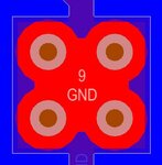
I have a surface mount component (8-pin soic) in altium with a thermal pad in the middle, the thermal pad in the footprint has 4 thermal vias in it. I need to connect these to my ground plane, but I'm getting several errors, and it wont connect. I'm getting Clearance Constraint Errors from the via to the pad, and short circuit constraint errors between the via and the pad as well. Does anyone know what I need to do to make these go away and have my via's connect to my ground plane? I'm attaching a pic

much thanks!
Capture.JPG
 

you need to assign the vias to the ground net as well. also make sure you do not have a via to pad rule that might give you the error.
 
you need to assign the vias to the ground net as well. also make sure you do not have a via to pad rule that might give you the error.

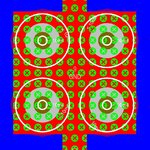
I'm not sure how to access the via's in order to assign them to the net, they are part of this component's footprint. I think the rule that keeps getting violated is the electrical clearance rule, I'm just using the default rules. On my ground plane it looks like this

Capture 2.JPG

thanks
 

just select the vias and right click mouse their in properties assign net name to vias (i.e. GND in your case).
Also you have to make "direct connect" option for vias if you want full contact of GND copper with vias.
 
I'm not sure how to access the via's in order to assign them to the net, they are part of this component's footprint. I think the rule that keeps getting violated is the electrical clearance rule, I'm just using the default rules. On my ground plane it looks like this

View attachment 69829

thanks

Hey, I know this is an old post but it's the only one describing the problem I've found from a quick google search.
At any rate, I found a way to access the vias in the thermal pad and thought I might as well add the solution to this thread for future googler's.
From what I understand of the problem it's that the thermal pad itself can have a net set on it, but the vias within it are stuck on "no net" and are unable to be selected for some reason.

Use the "Shift + V" key combination to explore through the violations when you're hovering over the component. This brings up a window of the component and all the "violating" pins/vias. From here you can expand each option and change the properties of the vias that were unselectable before (a quick right-click away)!

Hopefully that'll help someone else, and it wasn't just me not seeing any obvious solutions.
 
Wow! I thought I'd never see the day! A one-time post on this board that is NOT "Do my work for me plz send complete solution and documentation to wokkietokkie@lazybastard.com ASAP kthxbye! ^_^". And not just that, this is precisely the solution I was looking for too. :) Thank you Mr Shroomishness who will likely never see this!

I used the SHIFT-V + properties method first to see if it solved the violations. Which it did. :)

And for those future googlers looking for an even lazier solution, I came up with the following method.

Assume the QFN component is 'U1', and the thermal pad is pin number 33. Not an unreasonable assumption for a QFN-32 with thermal pad. ;)

Use the following query in PCB Filter: InComponent('U1') AND (IsVia OR (IsPad AND (Name LIKE '*-33')))

Apply filter, and verify that you indeed have now selected the thermal pad and the thermal vias.

Then go to PCB Inspector, and change Net to whatever value you need, GND for example.

Hopefully this helps one of those future googlers. :)
 
Status
Not open for further replies.

Part and Inventory Search

Welcome to EDABoard.com

Sponsor

Back
Top