Continue to Site

Welcome to EDAboard.com

Welcome to our site! EDAboard.com is an international Electronics Discussion Forum focused on EDA software, circuits, schematics, books, theory, papers, asic, pld, 8051, DSP, Network, RF, Analog Design, PCB, Service Manuals... and a whole lot more! To participate you need to register. Registration is free. Click here to register now.

[SOLVED] R-2R Layout for Process Gradient Elimination

Status
Not open for further replies.

mburakbaran

Member level 2
Member level 2
Joined
Jan 18, 2010
Messages
44
Helped
0
Reputation
0
Reaction score
0
Trophy points
1,286
Location
leuven
Visit site
Activity points
1,724
Hi everyone. I'm designing an R-2R DAC which has 8 bits. R=10k. I'd like to make it robust against process gradients. Any ideas on how I can realize that?

I've been checking Baker's book but it did not help me much...

There was this paper mentioning a "Quadrature Layout" technique in which the resistors are split into 4, but they did not give any more details about the implementation of the layout.

Thanks in advance.
 

well thanks mate. but i am confused about the method proposed in the second page of the document you've supplied. since i need about 25 of these resistors, how could i apply that to whole picture? If a group them two by two as proposed, they would match in pairs of two. but not all?? i guess you've got my point. thank you very much again.


I think a two-dimensional array could be meant, also called cross-coupled pair, or tiling, s. these 2 pages from
Akshay G: "Analog Layout Techniques in VLSI": View attachment 76871
 

If a group them two by two as proposed, they would match in pairs of two. but not all??

Such a "Quadrature Layout" contains 2 resistors. If you need 25 of them, you need at least 13 of these quadrants. So you can create an array of 1x13 , or 3x5 (or 5x3), or 4x4 of those quadrants, configuring the unused ones (if so) as dummies. Around the full array use further dummies in order to create the same "environment" for the outside quadrant cells.

The easiest build of course is the 1x13 array, needing just 2 dummies aside. Apart from the awkward 15:1 aspect ratio, this configuration suffers most from lateral gradient variation. More rectangular/square configurations provide better identity, but need more area, and routing connectivity is challenging.
 

How much process gradient do you really expect to get,
across the likely max layout dimension? I'd expect roughly
none on a 100x100um patch.

Now local photolithography effects (dummies) and thermal
effects (orientation, interleaving) could still be significant
at high bit counts. But I'd bet all of these are trivial against
major-carry errors, which is more about topology and how
the upper bits' structure / dependencies compare to the
lower.
 

Thanks a lot, really appreciated. I think I'll try to put them in a square like layout...
One more question though. As you pointed out, the routing is likely to be an issue. Since probably i ll be using different metal layers for routing, how much resistance deviation do you think this routing could bring? Is it considerable or not?


Such a "Quadrature Layout" contains 2 resistors. If you need 25 of them, you need at least 13 of these quadrants. So you can create an array of 1x13 , or 3x5 (or 5x3), or 4x4 of those quadrants, configuring the unused ones (if so) as dummies. Around the full array use further dummies in order to create the same "environment" for the outside quadrant cells.

The easiest build of course is the 1x13 array, needing just 2 dummies aside. Apart from the awkward 15:1 aspect ratio, this configuration suffers most from lateral gradient variation. More rectangular/square configurations provide better identity, but need more area, and routing connectivity is challenging.

- - - Updated - - -

I really dont have any idea on that.. This is the first time I am using 90nm TSMC, and I've never cared about gradients before (I was using 0.35um AMS in the past)...

How much process gradient do you really expect to get,
across the likely max layout dimension? I'd expect roughly
none on a 100x100um patch.

Now local photolithography effects (dummies) and thermal
effects (orientation, interleaving) could still be significant
at high bit counts. But I'd bet all of these are trivial against
major-carry errors, which is more about topology and how
the upper bits' structure / dependencies compare to the
lower.
 

Since probably i ll be using different metal layers for routing, how much resistance deviation do you think this routing could bring? Is it considerable or not?

Depends very much on the R-2R resistance value itself, of course: mΩ deviations would play some role in connecting resistances of the order of Ωs -- also because of different voltage drops due to different currents -- but surely not with R-2R resistances in the order of kΩs or even more.

Anyway I'd try and make the routing as symmetrical as possible, if not only for inspection facility reason.

If the current in the R-chain isn't insignificant, be aware that the chain current will increase towards the higher bits -- if these are active.
 
  • Like
Reactions: sohaee

    sohaee

    Points: 2
    Helpful Answer Positive Rating
There's another consideration for this particular application. Most advice regarding layout assumes you want all the components to be equally well matched. For the R-2R network this is not what you want.

Think about this: A 2% mismatch between the two most significant bits will have a much worse effect on the DAC's performance than a 50% mismatch of the least significant bit.

This suggests that it's worth aiming for extremely good matching of the resistors for the first few bits, at the expense of much worse matching for the last few bits.
 
Thank you very much Sir. One last thing, since there are Rs and 2*Rs in the core of the circuit, considering this quadrature method, how am i supposed to obtain matched Rs and 2Rs at the same time? My point is, I use R=10k, I'd firstly consider splitting this value to 4 which is 2.5k, and placing them in the axis in a symmetrical way whatsoever and then get their series combination right? Or is it wiser to use 40k s and route them in a parallel way? After the R values are matched, i figure I'd keep routing and obtain the 2Rs as well right?


Depends very much on the R-2R resistance value itself, of course: mΩ deviations would play some role in connecting resistances of the order of Ωs -- also because of different voltage drops due to different currents -- but surely not with R-2R resistances in the order of kΩs or even more.

Anyway I'd try and make the routing as symmetrical as possible, if not only for inspection facility reason.

If the current in the R-chain isn't insignificant, be aware that the chain current will increase towards the higher bits -- if these are active.
 

... since there are Rs and 2*Rs in the core of the circuit, considering this quadrature method, how am i supposed to obtain matched Rs and 2Rs at the same time? I use R=10k, I'd firstly consider splitting this value to 4 which is 2.5k, and placing them in the axis in a symmetrical way whatsoever and then get their series combination right?

I'd use R=2*5k , so you can get 2R (20k) in one square. For the single Rs, use one half of such an adjacent square.

Or is it wiser to use 40k s and route them in a parallel way?
No, this needs unnecessarily much area, and offers no advantage compared to the 2*5k (or 4*2.5k) serial configuration.
 

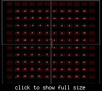
You've been very helpful Sir, thanks a lot. I couldn't really understand how 2R will be a square though. Could you please comment on the configuration in the attachment. I've placed resistors and numbered them. Every resistor is split into 4 as you can follow. I've assumed that the gradient will come in a linear manner both horizontally and vertically. I know that the distance between resistors is unnecessarily long but I'll fix it, just would like to get a comment on the general placement.


I'd use R=2*5k , so you can get 2R (20k) in one square. For the single Rs, use one half of such an adjacent square.


No, this needs unnecessarily much area, and offers no advantage compared to the 2*5k (or 4*2.5k) serial configuration.
 

I couldn't really understand how 2R will be a square though.
Use 2*5k per resistor, so you get two 10kΩ resistors or one 20kΩ in one square:
18_1341932616.png


Could you please comment on the configuration in the attachment. I've placed resistors and numbered them. Every resistor is split into 4 as you can follow. I've assumed that the gradient will come in a linear manner both horizontally and vertically.

I'd say a 10*10 array is a bit exaggerated if you can do it easily with a 4*4 array. Don't forget that linear gradients -- if existent -- increase variations linearly, eo ipso.

And you don't need a border of equal square cells around the array to guarantee a continuous environment: a full rpoly line around the array with the same width as your resistors, and as close as the DRC allows for, is enough.

For a successful LVS you probably need 2 contacts on this poly line, e.g. at 2 opposing edges, both connected to GND or VDD, which results in 2 parallel short-circuited dummy resistors for which you should install an equivalent dummy resistor in your schematic in order to satisfy the LVS.
 

Could you please comment on the configuration in the attachment. I've placed resistors and numbered them.
Can you show the DAC circuit and indicate which number corresponds to which resistor? Without this information, your picture is meaningless.
 

Every four resistor corresponds to 1 R=10k. They're split into 4. The numbering is kind of arbitrary, The first two 2Rs which is at the LSB section is realized via (number 1 + number 2)... You can follow the rest from the figure I've supplied.


Can you show the DAC circuit and indicate which number corresponds to which resistor? Without this information, your picture is meaningless.

- - - Updated - - -

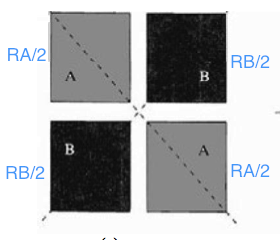
Dear Sir, The picture proposes a matching of two resistors A and B. The thing is, with this laying out how am I supposed to match the whole? My point is, let's say A and B are 10k Rs. Let's think of C and D which are also R=10k each. And this square box of C-D is placed next to the square of A-B. A and B seems to be suppressing gradients and matches them, also C-D does the job for them two. But How can you say that A-B vs C-D is also going to be matched?

Within the picture I've given, I tried to split everything into 4 and placed them in a symmetrical way for both axis. This should guarantee a very well defined R in my opinion. I just wanted to make sure that indeed it is? If not, please let me understand how I can do it with the way you suggested (4*4 array thing)... Thank you very much, sorry for bothering you over and over again.


Use 2*5k per resistor, so you get two 10kΩ resistors or one 20kΩ in one square:
18_1341932616.png


I'd say a 10*10 array is a bit exaggerated if you can do it easily with a 4*4 array. Don't forget that linear gradients -- if existent -- increase variations linearly, eo ipso.

And you don't need a border of equal square cells around the array to guarantee a continuous environment: a full rpoly line around the array with the same width as your resistors, and as close as the DRC allows for, is enough.

For a successful LVS you probably need 2 contacts on this poly line, e.g. at 2 opposing edges, both connected to GND or VDD, which results in 2 parallel short-circuited dummy resistors for which you should install an equivalent dummy resistor in your schematic in order to satisfy the LVS.
 

A and B seems to be suppressing gradients and matches them, also C-D does the job for them two. But How can you say that A-B vs C-D is also going to be matched?

Array matching. The quadrature matching A-B is continued in an array of squares which match just on a larger scale -- same principle, however.
 

Just to make things clear, Let's think of a 2 by 2 square and consider each letter is a 5k resistor:

A-C-D-B
E-G-H-F
F-H-G-E
B-D-C-A

And there are the axis between row 2-3 and column 2-3. Is this what you mean, sir?

Thanks a bunch again.


Array matching. The quadrature matching A-B is continued in an array of squares which match just on a larger scale -- same principle, however.
 

Status
Not open for further replies.

Part and Inventory Search

Welcome to EDABoard.com

Sponsor

Back
Top