Continue to Site

Welcome to EDAboard.com

Welcome to our site! EDAboard.com is an international Electronics Discussion Forum focused on EDA software, circuits, schematics, books, theory, papers, asic, pld, 8051, DSP, Network, RF, Analog Design, PCB, Service Manuals... and a whole lot more! To participate you need to register. Registration is free. Click here to register now.

How can I convert the bitstream of a simple sigma delta converter to a binay value?

Status
Not open for further replies.

userx2

Full Member level 3
Full Member level 3
Joined
Sep 19, 2008
Messages
173
Helped
2
Reputation
4
Reaction score
3
Trophy points
1,298
Activity points
3,067
Hello

Please let me know if this is the wrong forum for this question.

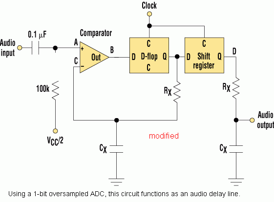
Can someone please explain to me (I am a complete novice in digital signalling and Sigma Delta converters), how to convert the PCM bitstream output from my converter to a conventional binary integer?

Someone mentioned to me the use of a counter but I am struggling to see how that can work.

I have seen all the mathematics but a simple explanation on "how to" would suit me a lot better.

At this stage, I want to convert / sample the output of a potentiometer.

I am using a D-FlipFlop with a comparator and RC circuit to produce the bitstream and I need to have the output as either 8 or 10 or 16bit values representing the level.


Best regards
2X
 

Seems to me you would need a counter AND a shift register.

You clock the counter & shift-reg with your sampling clock. Feed the bitstream into the shift register. When the counter hits 8/10/16 whatever - generate a pulse or edge. Then at this edge time, sufficient bits have been shifted in, and you can use this edge to "unload" the shift reg and latch the data into whatever is next in your circuit.

Naturally your shifter length should be >= whatever bit length you have chosen.
Also ... ummm.. you might need to reset your RC integrator with this same pulse/edge.

Hope this helps ?

Hello and thanks for the reply!
That is the bit I do not undertand. Counting pulses like that might be corect but it does just not compute in my old brain.
Something tells me that I need to convert pulse duration (or pulse width) into counts. The problem I have with this is that somehow, if I count pulses based on a bitstream, this all has to be synchronised to something?

What does this shift register do? Or is this from that presentation of some students who did something like this with a 6 bit counter? They called theirs a shift register, it was in actual fact a latch.
I was not able to figure out how their circuit really works because they do not explain how all those clock signals relate to each other. I thought it was pretty simple until I started rawing out a schematic :-(


Best regards
2X
 

From what I understand of your question, you essentially need to do a serial to parallel conversion. Off-the-shelf shift registers can do just that. Here is one example of an 8-bit shift reg ...
https://www.fairchildsemi.com/ds/74/74VHC164.pdf

Secondly, I am assuming from your description that you are generating a "digital" stream based on a circuit something like this :


The output of the comparator will be either high or low depending on the input voltage, & the previous voltage. I.e. the output indicates whether its a rising input or falling input.

Your DFF is then used to sample the comparators output at a fairly high speed resulting in a bit-stream which is a serial stream.

YOUR question was -- How to convert this 1-bit stream into parallel chunks of 8-bits each.

Here's what a Counter does (in this case used as a divider). It essentially 'counts' from 0 to N based on the input clock. When 8 clock edges have occured, then one of its outputs will go high.

YOu have to use THAT output to offload your shift register.

Thats it. Unfortunately I cannot explain it any more simplistically.

cheers & all da best !
 

Counting the number of '1' states over a defined time interval is identical to a first order CIC decimation filter. Usually a higher order filter would be used. You'll find many same topic threads about sigma delta and CIC at edaboard.
 

Counting the number of '1' states over a defined time interval is identical to a first order CIC decimation filter. Usually a higher order filter would be used. You'll find many same topic threads about sigma delta and CIC at edaboard.

Hello and thank to everyone for helping me here.

Are you esentially saying the following??? Please correct what I still have wrong...
1) To get an 8 bit output we need to count the highs on the itstream for 255 clock periods.
2) It does not matter where in the bitstream we start counting.

If the above is right, then I think I 've got it.


Because I didn;t understand this whole thing, I also came up with a different solution (theoretical so far):

I could get a PWM output going which has 255 steps (levels). It would run at high frequency, compared to the input from the potentiometer.
I can feed this to the comparator to compare to the intpu signal.
I could either sucessively approximate this or ramp it up until the the output of the comparator flips.
The 8 bit value in the PWM register at the point of flipping, would then be the output of the a/d converter.

Do you clever folks think that could work as well?
I guess I could stick with that bitsream method for now.

I want to do this in an FPGA as I need very many of these channels.
I need about 25 samples per second forat least 15 channels.

Best regards
X2
 

wow.

You guys don't understand the basics yet want to leap into FPGA across 15 simultaneous channels.

Good luck to YOU

LoL!
 
1) To get an 8 bit output we need to count the highs on the itstream for 255 clock periods.
2) It does not matter where in the bitstream we start counting.
That's basically correct, the '1' density is representing the input voltage. In contrast to a simple counter, a first order CIC decimator is working as an accumalator for fractional parts of the input signal, a signal of 0.5 LSB e.g. gives a a output for every second sample. A higher order CIC filters input and quantization noise and achieves a higher resolution.

Usually the decimation filter uses a power of two decimation factor, but that's not necessary.

You'll notice, that SD ADCs have effectively replaced classical slow ADC methods like dual-slope. That's mainly because of their better linearity, which doesn't depend on capacitor loss factors and similar. The oversampling aspect also involves less effort in analog filtering.

You guys don't understand the basics yet want to leap into FPGA across 15 simultaneous channels.
Good luck to YOU
LoL!
Hopefully you do understand it. Your suggested circuit doesn't work as a linear SD-modulator, it should use an integrator and the FF in the feedback loop.
Implementing a low resolution ADC is actually an easy task, and applying it to 15 channels in a FPGA design isn't more difficult than a single channel.
 

That's basically correct, the '1' density is representing the input voltage. In contrast to a simple counter, a first order CIC decimator is working as an accumalator for fractional parts of the input signal, a signal of 0.5 LSB e.g. gives a a output for every second sample. A higher order CIC filters input and quantization noise and achieves a higher resolution.

Usually the decimation filter uses a power of two decimation factor, but that's not necessary.

You'll notice, that SD ADCs have effectively replaced classical slow ADC methods like dual-slope. That's mainly because of their better linearity, which doesn't depend on capacitor loss factors and similar. The oversampling aspect also involves less effort in analog filtering.


Hopefully you do understand it. Your suggested circuit doesn't work as a linear SD-modulator, it should use an integrator and the FF in the feedback loop.
Implementing a low resolution ADC is actually an easy task, and applying it to 15 channels in a FPGA design isn't more difficult than a single channel.

you're a bit off-topic aren't you ? The circuit I posted was an attempt to capture the original question's details. Nothing to do with your clever linear SD modulator. Who asked about linear SD modulators anyhow ?!

cheers bro' !
 

The original question is about a SD modulator used as ADC, in so far we would assume linearity is an obvious requirement. Seriously speaking, I don't believe that the circuit from post #4 will produce accceptable results as shown. I rather guess there's a drawing error involved.

I also think, you shouldn't consider about "OT" after your post #7. It's not the usual style at edaboard to make pointless comments about the technical knowledge of other members. No matter if they seem to be substantiated somehow or pure invention, as presently.

P.S.: A more promising SD variant in my view

 
Last edited:

The original question is about a SD modulator used as ADC, in so far we would assume linearity is an obvious requirement. Seriously speaking, I don't believe that the circuit from post #4 will produce accceptable results as shown. I rather guess there's a drawing error involved.

I also think, you shouldn't consider about "OT" after your post #7. It's not the usual style at edaboard to make pointless comments about the technical knowledge of other members. No matter if they seem to be substantiated somehow or pure invention, as presently.

P.S.: A more promising SD variant in my view


IMHO your circuit presented is fearfully substandard, and reveals the fact that you have never actually WORKED with real opamps or comparators. I mean real hardware, not a Spice model.

About those "improvements" and "error corrections", have you ever actually tried feeding a comparator (or opamp) input via a cap coupling and no bias voltage ? I think not.

Secondly, shifting the 1st Rx to the output of the DFF doesn't make diddly difference to your "linearity" except that it reduces the overall shift-register delay by 1 clock. And also makes the response to input signal exactly that much slower. Just adds a phase delay, thats all. D-uh.

Regarding comments on (perceived/ sensed/ seen/ detected/ whatever) technical knowledge of others. I think that that IS a very important aspect of mentoring. Proper feedback rather than fake support. Much more useful. YOU want to give fake praise.... thats your choice.

Lets's stop this needless argument. The original poster has no idea what we're writing about anyhow.

cheers!
 

Seriously speaking, I don't agree about any of the above statements, except for the conclusion, that it's useless to continue the discussion.
 

wow.

You guys don't understand the basics yet want to leap into FPGA across 15 simultaneous channels.

Good luck to YOU

LoL!

Hey relax, just 'cause I am too old and rusty to uderstand the Sigma Delta converter mathematics doesn't mean I don't understand anything at all. I have been doing this for quite a while:)


I am currently investigating whether it would be feasable and cost eective to replace 15 seperate processors on one of my products with a single FPGA. If it looks favourible, I will do a prototype.

The Lattice MachOX eval board that I have here does not seen to bring out any reasonable number of IO pins so I don't think I can use that for doing more than a few basic test at all :-(

Regards
X
 
Last edited:

I think, it's not necessary to understand SD mathematics (particularly the noise shaping point) to implement a 1-bit ADC. I once designed an analog frontend for an analytical system using this method, at times when no suitable high resolution ADCs had been available. As I learned later, the performance could have been improved by applying SD theory.

You didn't tell much about the system specification. I would generally try with off-the-shelf ADC solutions. I'm doing a lot with FPGA, but mainly for problems that can't be handled by ready-made chips. Nevertheless it's instructive to learn about FPGA with hands-on.

Regards,
Frank
 

Status
Not open for further replies.

Part and Inventory Search

Welcome to EDABoard.com

Sponsor

Back
Top