Continue to Site

Welcome to EDAboard.com

Welcome to our site! EDAboard.com is an international Electronics Discussion Forum focused on EDA software, circuits, schematics, books, theory, papers, asic, pld, 8051, DSP, Network, RF, Analog Design, PCB, Service Manuals... and a whole lot more! To participate you need to register. Registration is free. Click here to register now.

[SOLVED] PFC Simulation (UCC28019)

Status
Not open for further replies.

daneloctober

Member level 2
Member level 2
Joined
Jan 28, 2011
Messages
52
Helped
2
Reputation
4
Reaction score
2
Trophy points
1,288
Location
Quezon City, Philippines, Philippines
Visit site
Activity points
1,708
Hello!!!

I was assigned to design a PFC circuit using the UCC28019 with the following specs:

Output power = 2.2kW
Output Voltage = 380 V
Input Voltage = 265 VAC
Input Voltage Frequency = 60Hz

TI has already been so helpful by providing a schematic in OrCad (which can be simulated using PSPICE) and a calculator for values of the essential components. All I had to do was enter the specs for my circuit and then the values would be adjusted accordingly.

My REAL problem is how to replace the BOOSTCCMDCM subcircuit (it comes with the downloadable UCC28019 sample schematic file) in the original schematic, with the actual boost converter components (a MOSFET and a diode). I attached pictures of the "ideal" (because of the presence of the BOOSTCCMDCM) and "realistic" schematics.

How come I'm only getting an output voltage below 100 when I replace the BOOSTCCMDCM thing with a mosfet and a diode as shown in the data sheet circuit???...

Here's the schematic and results with the BOOSTCCMDCM:
IDEAL.jpg
IDEAL wave.jpg

Here's the one without:
REALISTIC.jpg
REAL wave.jpg

And this is the schematic from the datasheet:
datasheet ucc28019 circuit.jpg
By the way, I'm using the OrCad 16.5 lite version.
 

A) In your circuit R33 (10K) is much too high and will slow the switching badly.
B) Are you sure fdc6322CN/FAI is a power MOSFET? When I Google "fdc6322", all I can find is a low power dual N & P Channel FET.
 

OK, something else came up. When I replace the switching transistor model with a power mosfet model, it stops becoming a PFC!!! What I mean is that the current spikes from the source remain.

ALSO, I will attach my sort of new schematic with the waveforms. I decided to retain the switching transistor model that T.I. provided. I don't UNDERSTAND the current spikes. The red waveform is the source current, the dark blue is the inductor current, the light blue waveform is the output voltage. PLEASE HELP!!! If I can't solve this, I will be consigned to think that it's a simulation issue and just go on with constructing the circuit.. >_<

Here's the waveforms:
2KW.jpg

Here's the schematic:
Transient _ 2KW.jpg
 

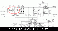
IMHO, you're getting current spikes at the input because you don't have a filter at the input. Note that the circuits in the datasheet all have input filters (circled in red below).

btw, EMI suppression and power factor correction are two separate issues.

 
It will help, but that's the least of your worries. Looking at your graphs, there's two main problems:

Firstly, the current draw in the first 300mS is ridiculous; if a circuit breaker doesn't trip in time, your circuit will burst into flames.

Secondly, after the first few hundred mS, when the circuit has settled down, the current draw at the input is horribly unsymmetrical, with a totally wrong waveform.

Getting back to the first few hundred mS, what is going on there? The output voltage jumps up almost instantly to about 450V, far above what it should be, then just sits there for 200mS without even any ripple. Meanwhile hundreds of amps of current are being drawn from the input. Where is that current going? As far as I can see, the switching transistor is shunting it straight to ground.

It would be useful to look at the gate voltage and the voltage on the right of the inductor to see what's going on with the switching.

The UCC28019 is supposed to provide PFC, soft start and overcurrent protection. Your circuit isn't doing any of those.
 
The UCC28019 is supposed to provide PFC, soft start and overcurrent protection. Your circuit isn't doing any of those.

EXACTLY why I'm going crazy over this infernal piece of encrypted model (no offense T.I. lol). I actually tried to run the basic circuit they gave, which was just a 300+W PFC (mine is for 2.2kW, if you would recall) and I got similar waveforms. I'm guessing this anomaly has something to do with the model being "averaged"?... Cause you won't see 65kHz switching. I just saw about 120Hz at the most. Oh well. This is just what I'm going to do. I'm going ahead with my design and trust that it will work because I followed the design procedure to the best of my ability. Which isn't much. Haha!

Thanks so much for your comments! I'll update you on the results. =D
 

So their Spice model is simplified to the point where you can't even see the 65KHz switching? Yech! How are you supposed to check switching times, MOSFET dissipation etc with that? I was wondering what that "BOOSTCCMDCM" black box was all about.

edit: I see here on the TI website, there's a PSpice transient model as well as the PSpice average model. Maybe that would be more useful.
 
Last edited:
Yep, that's what I used. Hehe.

Anyway, thanks for really trying to help godfreyl. I asked TI directly in their forum about the whole thing and this is their answer:

A few points about the model:

1. The UCC28019 transient model is really an "Average" model that is used to test the transient features of the part. In this model, all the switching nodes have been removed and replaced with the average waveform at that node. This is required to run the simulation till ~ 2 seconds. As a result, you will not see any switching waveforms in the result.

2. The BOOSTDCMCCM block is the average model for the BOOST transistor and its interface to UCC28019 and is required for the model to function properly.

3. Startup has not been modeled in this Average Model, so please ignore the first 500ms - 1sec of the waveform as that time is required to reach the steady state.

4. The model has been tested for the 350W EVM application only. When I ram your 2.2kW application circuit, I saw distortion. However, if I reduce R23 from 30m to 20m then the distottion goes away.

Soooo... I guess I'll just go ahead with my design. Again, THANK YOU!!! =D
 

Status
Not open for further replies.

Similar threads

Part and Inventory Search

Welcome to EDABoard.com

Sponsor

Back
Top