Continue to Site

Welcome to EDAboard.com

Welcome to our site! EDAboard.com is an international Electronics Discussion Forum focused on EDA software, circuits, schematics, books, theory, papers, asic, pld, 8051, DSP, Network, RF, Analog Design, PCB, Service Manuals... and a whole lot more! To participate you need to register. Registration is free. Click here to register now.

High frequency design pcb

Status
Not open for further replies.

spman

Advanced Member level 4
Full Member level 1
Joined
Aug 15, 2010
Messages
113
Helped
0
Reputation
0
Reaction score
0
Trophy points
1,296
Visit site
Activity points
2,061
High frequency design

Hi

I want to drive a SDR SDRAM with Spartan3 fpga. According to datasheet the clock of RAM is 100 mhz. So the frequency is high and i'm not sure about PCB.
Should i be careful about PCB design? What is the rules should be considered in PCB?

My another questions is about the RAM. Is it possible drive it with lower frequency? If possible, how much is the maximum frequency that i can design PCB without troubles.

thanks.
 

Hi,
Have you checked PCb/Layout design guidelines for the SDRAM?
Few General rules for PCB routing-
1. Segragate the zones of high speed , Low Speed & power signals/ components.
2. Group data, address and control signals as per recommendation. ( A data byte always associate with strobe and mask signals)
3. A group should have matched length while routing.
4. No other signals should cross the layers except memory signals including pwr & ground.
5. Trace width requirement depends on the current ratings.

Follow the Basic rules.

Hope this is useful.
 
Hi Spman!
I agree with Shashi. hope you got the answer for first questions.
The answer for your second question is "you can drive it with lower frequencies also by controlling/configuring the frequencies in software". PCB routing and other constrains will not come into picture if you follow the answer for the first question. Also the minimum frequency depends on the memory device and processor/controller. please go through the corresponding datasheets once again. all the best.
 
  • Like
Reactions: spman

    spman

    Points: 2
    Helpful Answer Positive Rating
Thanks friends

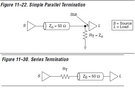
I understood that i must use a signal termination scheme. I found two easy solutions.
1- Single parallel termination
In a simple parallel termination scheme, the termination resistor (RT) is
equal to the line impedance. Place the RT as close to the load as possible
to be efficient (see Figure 11–22).
The stub length from the RT to the receiver pin and pads should be as
small as possible. A long stub length causes reflections from the receiver
pads, resulting in signal degradation.
2- Series termination
In a series termination scheme, the resistor matches the impedance at the
signal source instead of matching the impedance at each load (see
Figure 11–30).
45_1334223822.jpg


I doubt first solution. Won't voltage be divided? It seems one half of the voltage will receive to the load. there is another problem. the impedance of tracks is too low. How it assumed 50 ohms in the figure?!! The impedance of tracks hardly reaches to 2 ohms!
And what about bidirectional signals such as data bus? What end must the resistor be fixed?
 
Last edited:

May anyone give me a sample schematic and PCB including FPGA and SDR SDRAM (no DDR) please?
 

Thanks friends

I understood that i must use a signal termination scheme. I found two easy solutions.
1- Single parallel termination

2- Series termination

45_1334223822.jpg


I doubt first solution. Won't voltage be divided? It seems one half of the voltage will receive to the load.
That's correct, but there is not a reason to doubt the solution. The driver will need to be able to drive a 50 ohm load.
there is another problem. the impedance of tracks is too low. How it assumed 50 ohms in the figure?!! The impedance of tracks hardly reaches to 2 ohms!
Impedance is a function of frequency. The 'hardly 2 ohms' that you're talking about is a DC value, something you would measure with a meter. The 50 ohms is an AC value, the value that the driver sees when it is trying to change the voltage level of a signal. This is a function of track width, distance to the nearest plane and the PCB laminate material. 50 ohms is a fairly typical value for common circuit boards.
And what about bidirectional signals such as data bus? What end must the resistor be fixed?
You should consult the datasheet for specifics, but many times putting the termination resistor (series or parallel) in the middle of the net is all that is needed. One could also terminate at both ends, but that's likely not appropriate for a trace that is only a couple of inches long and not terribly high speed.

Kevin Jennings
 
I want to point out that what's important is edge rate, not the clock rate.
Also, the distances from the drivers to the receivers of your circuit are important.
If you have access to signal integrity simulation tool such as Hyperlynx, it would be good idea to model the transmission and simulate it. If you don't, I recommend to read Dr. Howard Johnson's "High Speed Digital Design". it tells a lot about transmission line theory.
 

Status
Not open for further replies.

Part and Inventory Search

Welcome to EDABoard.com

Sponsor

Back
Top