Continue to Site

Welcome to EDAboard.com

Welcome to our site! EDAboard.com is an international Electronics Discussion Forum focused on EDA software, circuits, schematics, books, theory, papers, asic, pld, 8051, DSP, Network, RF, Analog Design, PCB, Service Manuals... and a whole lot more! To participate you need to register. Registration is free. Click here to register now.

[SOLVED] Any advice in pic 18f4550 developement board?

Status
Not open for further replies.

electrodarkness

Member level 1
Member level 1
Joined
May 2, 2010
Messages
39
Helped
0
Reputation
0
Reaction score
0
Trophy points
1,286
Location
Ganesti, Transylvania, Romania
Activity points
1,649
I've recently built a Dev-board in Eagle Cad with a pic18f4550 core, and I'm curious if the design can be optimized further ( rooting, component placing) since this is my first major project with smt devices. Any advice, opinion would be really appreciated ( the Eagle files are attached below).
 

Attachments

  • proto.zip
    90.3 KB · Views: 131

I suggest you to put this project on the forum in pdf or image format. More people will look at it, as not everyone have Eagle installed.
 

This can be optimized at least for half or 1/3.


Original files as images:
pcb.pngsch.png


Use double layer!
 
As it is development board, size is not critical. In my opinion current size is quite good.
Power supply paths should be wider and ground should be placed in free fields (ground polygons). Remember to put 100nF capacitor close to each power supply pin pair of the microcontroller.
 
Hi,

Your ICSP PGD and PGC lines are wired incorrectly - you have put them to pins 39 and 40 like on a DIL chip, the SMD version is to pins 16 and 17.

If you are using smd then why use a standard led ?

If you are hand soldering its often better to select a larger size smd part and allow plenty of space around them.
 
Thanks for pointing out the ICSP. As for the LEDs I thought that the smt devices are on the bottom, and the pin rows at the top( because I don't have any smt pin rows), then the LEDs should be on the top also to see them.
 

You can use standard led no problem, just solder on top side. Pay attention on overlap J1 and D1 (power connector and diode).

Development board can be big, but You should practice on every PCB You make. Each next PCB should be better then the last.

You should practice double side PCB, space optimization, ....

SMD used to make PCB smaller not like DIP!!!
 

Thanks for pointing out the ICSP. As for the LEDs I thought that the smt devices are on the bottom, and the pin rows at the top( because I don't have any smt pin rows), then the LEDs should be on the top also to see them.

Hi,

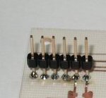
On many commerical boards the smd components and pin headers are on the same side of the board, its easier to mount and protect the board with things on just one side.

You can easily solder standard 0.1" headers to a smd board, once its soldered on you can usually push the black body down the pins so it does not look so obvious.
 

Attachments

  • conn.jpg
    conn.jpg
    38 KB · Views: 159
Updated PCB with correct ICSP connections and thicker power wires. wp100 then I think I should go to one sided-only soldering. Thank you guys for your help.
 

Attachments

  • proto.pdf
    37.8 KB · Views: 130

Its not wront to do this as single side PCB, and next board also single side, and next, and next also, but when you go to make next You will say this I make double sided. Nothing is wrong with single sided.
 

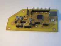
I had some time to make some photos of my pic development board, it works great. I've programmed it twice or more, now I'm thinking of some sort of boot loader, but the provided Microchip boot loader won't compile in Mplab X due to some errors.
 

Hi,

Nice work !


Perhaps post your schematic and pcb design for others to try..?

Afraid I cannot help with MplabX or the bootloaders but sure some of the other guys will help ..
 

Hi,

Just one question, I really do not know USB and all its parameters / options, but pin 37 VUSB is not connected to anything, most circuits I have seen usually have it connected to a capacitor to ground ?
 

Thanks for mentioning! Pin Vusb is usually connected to a capacitor with 100-470 nF capacitance to ground. I've used a 330nF 806 smd capacitor, but I forgot to correct on pcb.
I've uploaded the corrected version. I'm nearly done with the boot loader in MikroC because I'm not used to Mplab, I will post the hex file soon.
 

Attachments

  • protoI.pdf
    2.7 MB · Views: 158
Last edited:

Now I have a little spare time, so I post the boot loader(in .txt format) . The device can be programmed with MikroC HID utility after reset.
 

Attachments

  • boot_proto.txt
    19.2 KB · Views: 119

Status
Not open for further replies.

Similar threads

Part and Inventory Search

Welcome to EDABoard.com

Sponsor

Back
Top