Continue to Site

Welcome to EDAboard.com

Welcome to our site! EDAboard.com is an international Electronics Discussion Forum focused on EDA software, circuits, schematics, books, theory, papers, asic, pld, 8051, DSP, Network, RF, Analog Design, PCB, Service Manuals... and a whole lot more! To participate you need to register. Registration is free. Click here to register now.

Offset problem with instrumentation amplifier and RF detector source

Status
Not open for further replies.

Waveco

Newbie level 4
Newbie level 4
Joined
Oct 16, 2008
Messages
7
Helped
0
Reputation
0
Reaction score
0
Trophy points
1,281
Location
Spain
Activity points
1,376
Hello everybody,

I'm facing some offset problems with an instrumentation amplifier circuit. I'm using it to amplify the 'quasi-DC' signals from a RF detector composed by a dipole antenna and a schottky diode. The schematic is the following:
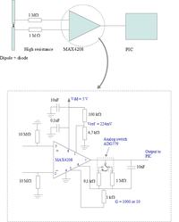


The connection between the diode and the instrumentation amplifier consists of two resistive lines of 1 MΩ.
I have chosen the MAX4208 instrumentation amplifier as it has very (ultra :wink:) low input offset voltage (Vios), input bias current (Ib) and input offset current (Ios). Typical specs for 5Vcc and 25 ºC are: Vios = 3 µV. Ib = 1 pA. Ios = 1 pA. Considering these specifications I expected, quite naively, not having any major problem concerning the offset.
From my calculations, I should have an offset = G * (Vios + Ios*(source impedance/2)). For a G=1000 value: offset = 1000 (3µV + 1pA*(2MΩ + 500kΩ)/2) ≈ 5mV.
However, for a gain = 1000 configuration, I'm getting a negative offset of around 100 mV.
Some clues from the tests I have done:
- For a gain = 10, there is no output offset
- The offset value varies with the resistive lines resistance value.
- The offset shows a great dependence on temperature variations (as a result of scohttky diode junction resistance variation with temperature, I guess)

Any idea on the cause and how to eliminate this offset?

Thank you!
 

Does the oscilloscope confirm that the output is really DC?
What happens if you put some capacitors in parallel to the 10Mohm resistors?
Maybe some RF gets (partially) rectified by the input stage of the amplifier ...
 

The detector would charge-pump with any input signal, the
magnitude of resulting voltage depending on the input power.
I'd start with trying out the high gain setting with the input
shorted (maybe at the detector, and the inboard side of the
1Mohm lines, both, just to see whether it follows Vin or Zin
more).
 
  • Like
Reactions: Waveco

    Waveco

    Points: 2
    Helpful Answer Positive Rating
Instrumentation and other opamps tend to increase the offset when the input resistance is high as well as the gain. I do not see why you use the two 1 MOhm resistors at the input. To filter any RF, using 10 kOhms is enough, and put a 10 nF capacitor across the input lines. You can also divide each resistor in two 5 kOhms and connect the capacitor at this half-way.
 

dave9000:
The offset appears when the circuit is not excited by any field (I test it in an anechoic chamber). So with no input signal, I get a -100 mV (approximately) offset at the output.
Therefore it's not about RF picking-up. In fact the lines do have a filter to eliminate RF signals, but I forgot to include it in my schematic. You can see the actual schematic here below:


Jiripolivka:
The resistive lines are used to move the detector away from the electronics, in order to not perturb the RF signal being measured. These lines are some 15 cm long, and they must have a rather high resistance so they don't perturb the signals being measured, nor pick up RF signals. So high resistance source is one of the difficulties we have to struggle with in this design.

dick_freebird:
I will do these tests and i'll be back with the results.
DONE!
- For a gain = 10, there is no output offset
- The offset value varies with the resistive lines resistance value.
- The offset shows a great dependence on temperature variations (as a result of scohttky diode junction resistance variation with temperature, I guess)
- When the input is shorted at the detector (the diode is shorted) the offset is somewhat smaller.
- When the input is shorted after the resistive lines, at the amplifier inputs, there is no offset.
- The 10 MΩ resistors used to provide an input bias current return path seem not to have any effect in the circuit behavior. The behavior is the same with or without these resistors.


Thank you!
 
Last edited:

I would stress again that at high gain setting, offset is quite often more annoying. I would advise the following:

Use two detectors connected "against each other", in series, between opamp inputs. Keep one close to the opamp and "in dark" from any radiation. The other, in the dipole, will pick up and rectify signals. A similar approach is used in precision thermometer sensors.
Use two opamps cascaded with lower gain setting; if needed, an offset suppression signal can be driven in the second stage.
Try an isolation opamp, with optical fiber carrying detector output to the "main" amplifier. Then there will be no disturbance by "wires" to the tested field. See Narda website, they do it that way. You can even use the same fiber to send the DC power to the first opamp (the output signal is audio).

---------- Post added at 18:15 ---------- Previous post was at 18:11 ----------

From the last three blue points above I can see that the two large resistors in series with detector do cause the offset. Try reducing them as I wrote, to ~10 kOhms.
Test the circuit as is, with no diode but a 100 k resistor, at a full gain, and vary the ambient temperature. Find what drives the offset and replace it, or compensate.
 

I still didn't hear about any oscilloscope measurements. Did you check that there are no low frequency signals possibly overloading the amplifier, e.g. 50 Hz hum?
 

Instrumentation and other opamps tend to increase the offset when the input resistance is high as well as the gain. I do not see why you use the two 1 MOhm resistors at the input. To filter any RF, using 10 kOhms is enough, and put a 10 nF capacitor across the input lines. You can also divide each resistor in two 5 kOhms and connect the capacitor at this half-way.

I agree, why not two 1 K resistors? 1 M just gives rise to all sorts of op amp bias issues as well as inherent thermal noise.

Also, why is there no capacitor across the two op amp inputs? If the whole purpose is to rectify they RF voltage into a DC voltage and amplify it, why is there no 10,000 pF capacitor to hold the charge?

Also, you are using this op amp with a single supply voltage, but you are incorrectly DC biassing the input ports to ground with those 10 M resistors. You probably need to bias the inputs to +2.5 V thru a divider, or run the op amp off of a dual DC supply.
 

Also, you are using this op amp with a single supply voltage, but you are incorrectly DC biassing the input ports to ground with those 10 M resistors. You probably need to bias the inputs to +2.5 V thru a divider, or run the op amp off of a dual DC supply.
I guess, every analog guy will be asking this at first sight. The MAX4208 has a small common input headroom of 0.1 V below negative rail, it shouldn't be completely absorbed by the bias current voltage drop across input resistors. But it will be by any unexpected common mode signal.

The connected antenna is apparently floating, why not bias the inputs to safe mid supply?
 
Hi everybody,

Concerning the 1 Mohm resistance, I cannot reduce this resistance because of the application. Indeed, it should be even higher!
In fact, these two resistances are two parallel, 15 cm long resistive lines, whose resistance is distributed along the line. They behave as a resistive transmission line, with a small intrinsic capacitance between the lines. The lines act as a low pass filter with a cutoff frequency of some kHz. No capacitor between the lines is then needed for rectification.

Therefore, the circuit must work with this high impedance. So the question would be: is the offset inherent to the high gain, high impedance source setting? Nothing can be done to reduce or get rid of the offset?
If that's so, I guess that one solution would be to use two cascaded amps with lower gain setting, as suggested by jiripolivka.

Concerning the inputs bias, I bias the input ports to ground as the input coming from the detector will always be positive. Also, this gives a greater output dynamic range (0-5V instead of 0-2,5V). However I'm not at all an expert in op amps (I think it's obvious :sad:) and don't know if it would be necessary to bias the inputs to the mid supply. Anyway, if I do so, will this modification affect or improve the offset problem?


With the high gain, the floating "long" line to the dipole and dipole itself calls for the offset problem. As the others advised, the easiest solution may be to connect a 1 MOhm potentiometer between Vcc and ground, and pull the both (or at least one) input pin to ~ Vcc/2. If you still see an offset, adjust the ~ Vcc/2 to get rid of it.

As the line from the dipole-/detector to opamp is so long, it will almost certainly pick up some static and RF signal from around (even light adds up), and can cause the offset. Did you tested the dipole detector alone with an oscilloscope? Maybe you will be shocked what you can see! Then no wonder you have an offset at the high gain!
 
  • Like
Reactions: Waveco

    Waveco

    Points: 2
    Helpful Answer Positive Rating
With the high gain, the floating "long" line to the dipole and dipole itself calls for the offset problem. As the others advised, the easiest solution may be to connect a 1 MOhm potentiometer between Vcc and ground, and pull the both (or at least one) input pin to ~ Vcc/2. If you still see an offset, adjust the ~ Vcc/2 to get rid of it.

As the line from the dipole-/detector to opamp is so long, it will almost certainly pick up some static and RF signal from around (even light adds up), and can cause the offset. Did you tested the dipole detector alone with an oscilloscope? Maybe you will be shocked what you can see! Then no wonder you have an offset at the high gain!

As for the signal picking up in the lines, I'm quite sure of avoiding this problem as I do the tests in electromagnetic field free environments: a TEM cell and an anechoic chamber. And the results are the same in both cases. So I don´t think that is the source of the offset.
Certainly the lines can pick up RF field. In fact I have already faced that problem, that's why I filter the amplifier input using 3 capacitors.

Concerning your advise of biasing the inputs to Vcc/2, I will do the test. However, I had rejected this option at the beginning of the development since it reduces a lot the output swing of my circuit: as the input is always positive, the output would only swing between 0 and 2.5 V, instead of 0 to 5 V. Am I rigth?
 

it reduces a lot the output swing of my circuit: as the input is always positive, the output would only swing between 0 and 2.5 V, instead of 0 to 5 V. Am I rigth?
no, you "limit" the input swing to +/-2.5V. The output swing will be from Vref to Vcc - something.
 

no, you "limit" the input swing to +/-2.5V. The output swing will be from Vref to Vcc - something.

Ok, I see. I'm just rising the common mode voltage up to 2.5 V. Thanks!
 

In fact, the input voltage won't be "always positive", because the diode is representing a differential voltage source, raising the anode terminal above zero and pulling the cathode terminal below, possibly outside the -0.1V input voltage range.
 
  • Like
Reactions: Waveco

    Waveco

    Points: 2
    Helpful Answer Positive Rating
Thank you again!

Last question concerning this subject: Are the 10 MΩ resistors providing the input bias current path really necessaries in this setup? If so, is the 10 MΩ value correct or could it be higher (using a higher resistance value would increase the amplifier input impedance...)?
 

Assumed you want to utilize the diode as zero bias detector, you would rather connect a low kohm load resistor. Otherwise, the diode operation is rather undefined and leakage currents play an important role. But I don't know about your diode detector and matching design.

Looking primarly at the amplifier, it can tolerate higher input bias resistors, but should use a mid supply bias to give higher margin for common mode voltage. Also input offset currents are "amplified".
 
Status
Not open for further replies.

Similar threads

Part and Inventory Search

Welcome to EDABoard.com

Sponsor

Back
Top