Continue to Site

Welcome to EDAboard.com

Welcome to our site! EDAboard.com is an international Electronics Discussion Forum focused on EDA software, circuits, schematics, books, theory, papers, asic, pld, 8051, DSP, Network, RF, Analog Design, PCB, Service Manuals... and a whole lot more! To participate you need to register. Registration is free. Click here to register now.

How to design Folded Cascode OTA with gain-boosting?

Status
Not open for further replies.

yonzzan

Junior Member level 3
Joined
Dec 12, 2006
Messages
26
Helped
0
Reputation
0
Reaction score
0
Trophy points
1,281
Visit site
Activity points
1,522
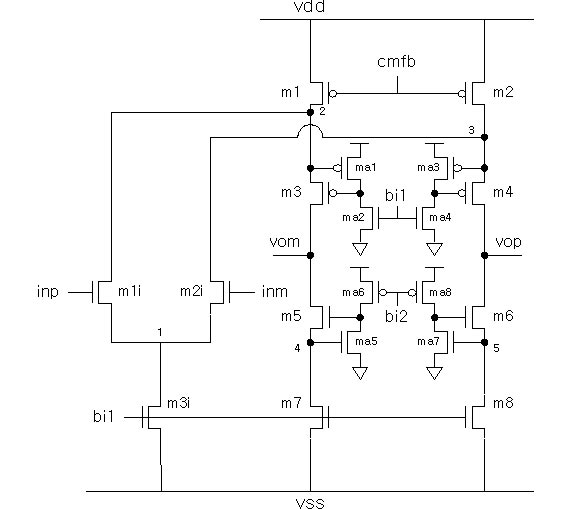
58_1171481470.jpg


I will really appreciate it, if you could give me advice about

1.how to determine its amount of current flowing through each transistor,
2. effective voltages(Vdsat, Vov, or Veff) and bias voltages(Vb1, Vb2, Vb3, Vcm)
3. its small signal gain.


Thanks

Added after 1 minutes:

The specification is below:
TSMC 0.18 micron technology
DC gain:60dB
Gain bandwidth product:500MHz
Phase Margin: 60
Output swing: 1v P-P
Output Load: 2pF
Slew rate: 20v/usec
fully differential..
 

Hi..
You can check Razavi for a brief view. The current could be fixed depending on the power constraints,slew rate constraints and the next block you are giving this output to(pushing equal current densities might be helpful if you want to maintain a vgs,for example).
Also the current in m1,m2 must be around 1.5 times that of the current in the diff pair,in order that the current through the cascode legs will not fall to 0 or a low value.
You can assume a similar vdsat for the cascodes and design taking care of the i/p o/p swings,and if there are any discrepancies you can adjust those values. Generally this architecture is used when there is a high vdd,say 3.3v. So,you won't have much of that problem unless otherwise,you need a relatively large swing.
 

Status
Not open for further replies.

Part and Inventory Search

Welcome to EDABoard.com

Sponsor

Back
Top