skn96
Junior Member level 3

Hello All
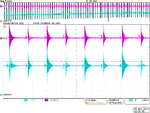
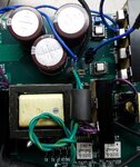
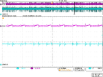
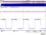
I’m working on a phase shifted full bridge dc/dc power supply prototype right now. The converter has been designed for 800W continuous power and must regulate for max 2 seconds of 2400W over load. The input is 400V coming from external power supply for now (later from PFC) and the output is 170V in complementary fashion i.e. +85V/-85V. Schematic has been attached. I anticipated ringing due to the use of 400V secondary diodes and I have added enough snubbers as you can see in attached schematic to solve it. I do not have a major problem with that . I have used very fast 650V Infineon mosfets from CFD2 series to make sure I have no problem with mosfet diode reverse recovery. My problem right now is the ringing on the input side of the converter due to the discontinuous nature of input current in full bridge convetrer. The current sensor CS1 is on the secondary side close to controller so I had to use a 16 Gage wire 20 cm length as loop so that current can be sensed by current sensor(CS1) which is located on the secondary. Wire loop starts form TP211 goes to secondary and come back and ends at TP201. I have twisted this 20cm wire but still it has some parasitic inductance contribution on the input side which is added to the parasitic already there from PCB traces. At power level above 200 W I do not have that much problem with ringing which is caused by input side parasitic inductance and mosfet capacitors. Picture 1 shows the input current waveform which is conducted through the wire loop. The voltage of drain to source for switches Q201 and Q200 has been shown also with no major ringing on top o them. But at very low load since the mosfet capacitors are not discharged before switching and there is no ZVS , enough energy for the ringing around 10Mhz is available as you can see in second picture. Obviously the effect of this ringing on the drain to source voltage of Q201 and Q200 is bad and very close to Mosfet voltage raining which is 650V. Now the question is how to eliminate this 10Mhz ringing on the input? I’ve heard people use saturable reactors and ferrite rings. I have no experience with suppressing these kind of ringing. Can you please help me with that?
I’m working on a phase shifted full bridge dc/dc power supply prototype right now. The converter has been designed for 800W continuous power and must regulate for max 2 seconds of 2400W over load. The input is 400V coming from external power supply for now (later from PFC) and the output is 170V in complementary fashion i.e. +85V/-85V. Schematic has been attached. I anticipated ringing due to the use of 400V secondary diodes and I have added enough snubbers as you can see in attached schematic to solve it. I do not have a major problem with that . I have used very fast 650V Infineon mosfets from CFD2 series to make sure I have no problem with mosfet diode reverse recovery. My problem right now is the ringing on the input side of the converter due to the discontinuous nature of input current in full bridge convetrer. The current sensor CS1 is on the secondary side close to controller so I had to use a 16 Gage wire 20 cm length as loop so that current can be sensed by current sensor(CS1) which is located on the secondary. Wire loop starts form TP211 goes to secondary and come back and ends at TP201. I have twisted this 20cm wire but still it has some parasitic inductance contribution on the input side which is added to the parasitic already there from PCB traces. At power level above 200 W I do not have that much problem with ringing which is caused by input side parasitic inductance and mosfet capacitors. Picture 1 shows the input current waveform which is conducted through the wire loop. The voltage of drain to source for switches Q201 and Q200 has been shown also with no major ringing on top o them. But at very low load since the mosfet capacitors are not discharged before switching and there is no ZVS , enough energy for the ringing around 10Mhz is available as you can see in second picture. Obviously the effect of this ringing on the drain to source voltage of Q201 and Q200 is bad and very close to Mosfet voltage raining which is 650V. Now the question is how to eliminate this 10Mhz ringing on the input? I’ve heard people use saturable reactors and ferrite rings. I have no experience with suppressing these kind of ringing. Can you please help me with that?


