Continue to Site

Welcome to EDAboard.com

Welcome to our site! EDAboard.com is an international Electronics Discussion Forum focused on EDA software, circuits, schematics, books, theory, papers, asic, pld, 8051, DSP, Network, RF, Analog Design, PCB, Service Manuals... and a whole lot more! To participate you need to register. Registration is free. Click here to register now.

Help with step down 48V to 12V!!

Status
Not open for further replies.

gumattos

Member level 1
Member level 1
Joined
Jan 3, 2017
Messages
36
Helped
1
Reputation
2
Reaction score
1
Trophy points
8
Location
Brazil
Visit site
Activity points
337
Hello guys, I'm new in the forum, and after searching a lot through the web and here in the forum, I've decided to post a new thread since I think I'm still missing something here.

So, I want to convert from 48V to 12V using a DC/DC converter, I found a lot of things on Internet but the circuit I made is getting 65% efficiency and it sounds bad. The original ciruit is from Roman Black and I am open for suggestions of new projects, the only change I made was replacing the original transistor from a BC327 to a TIP127, yes I know TIP127 is very slow and I do think that's the problem, but since I will work with about 0,6A I needed a Darlington transistor. I am accepting any kind of help and suggestions, sorry for the bad english.

Some considerations:

I will make a good number of these circuits, about 20 or 30, my dad will need them to get some cameras working, so no expensive stuff.

The circuit will directly on the sun (the extremely hot brazillian sun), that's why I need to use a TO-220 transistor (with heat sink) and need efficiency.

In Brazil a P Channel MOSFET good for switching can cost 12 times more than a TIP127, however if you think there is a way to make it work with MOSFET I am willing to try, just remember that a comparator or Op Amp maximum voltage is 36V

I am looking for something like 80% efficiency, but anything better than my actual situation will help.

Today with the 65% efficiency things are getting pretty hot under the 104 degrees sun.

Capturar.PNG
 

Have you looked at what's out there for "telecom" (48V
standard in USA) DC-DC "bricks"? There's a huge pool
of them and pretty competitive pricing, probably less
than your parts kit (let alone labor). Unless the journey
is the destination.
 
Have you looked at what's out there for "telecom" (48V
standard in USA) DC-DC "bricks"? There's a huge pool
of them and pretty competitive pricing, probably less
than your parts kit (let alone labor). Unless the journey
is the destination.

Hello dick_freebird, I already searched for these, but in Brazil they are hard to find, so the only alternative is importing from USA, and that's is a problem since my country have about 200% taxes for importing.

- - - Updated - - -

Have a look at these threads regarding this type of regulator:

https://www.edaboard.com/threads/330573/
https://www.edaboard.com/threads/331961/

E-Design, your suggestions helped very much, I just have one doubt, in this circuit:


You use the TL431 after the emitter from the transistor (with the resistors of course), can I replace this TL431 with a Zener Diode? I won't need precision on the output voltage and I don't have quick access to any TL431 for testing, can I replace it for a zener and remove the resistors? If I can, what voltage Zener should I use? I am using OrCad but the simulation is not working, I tried Multisim too but no sucess...
 

You can try out this revised circuit. This is not tested in the lab, but simulation looks promising.

I built a very similar circuit to this one that you simulated, but my simulation didn't worked, I tought I was doing something wrong but it's just my OrCaD apparently. Thanks again E-Design, I will try to fix my problem with OrCaD since the cuicuit is working. I will post the results as soon as I can!

One last thing, what simulation software do you use?
 

You can try out this revised circuit. This is not tested in the lab, but simulation looks promising.

This was done with TINA by Designsoft. I also checked it with SIMetrix and got similar resulsts.

- - - Updated - - -

Here are the results between TINA and SIMetrix.
 

Attachments

  • buck_48_comp.png
    buck_48_comp.png
    98.6 KB · Views: 224
  • step_load.png
    step_load.png
    39 KB · Views: 192
You can try out this revised circuit. This is not tested in the lab, but simulation looks promising.

This was done with TINA by Designsoft. I also checked it with SIMetrix and got similar resulsts.

- - - Updated - - -

Here are the results between TINA and SIMetrix.

E-Design, I tested the circuit here, in the first try It was a sucess, I don't have an oscilloscope right now so I can't make more analysis, but it was working great. Then I turned te circuit off, with the load of 0,5A and I removed the Vin wires. When I plugged the circuit back my NPN transistor burned up, alongside with the voltage reference zener. Then with some experiments I discovered there is a short that goes through the both transistors and through the reference zener. I changed components and checked connections, but from this first burn up every try was an instant short. I had only 3 NPN and 2 PNP so I will try to buy more tomorrow (here in Brazil the shops are already close). Anybody have any ideas, can the MOSFET be the problem, or any capacitor that is not working correctly?

Details:

The circuit is identical to E-Design's, the only changes were using BD138 and BD137, SB360 as Schottky and to replace the 1N914

I made the circuit on a breadboard, it can be some connection that got wrong after the first test, but I don't think that's probable.

Tomorrow I will buy everything new and a real board I can solder the components.
 

Those larger transistors may alter the switching characteristics of the circuit due to slower switching speed and gain.

You can add the components shown to have a more controlled switch-on transient response and some protection around the two transistors.

Without C4, there can be some unacceptable overshoot in the initial output voltage at turn-on.
 

Attachments

  • buck_48_mod.png
    buck_48_mod.png
    61.5 KB · Views: 186
Those larger transistors may alter the switching characteristics of the circuit due to slower switching speed and gain.

You can add the components shown to have a more controlled switch-on transient response and some protection around the two transistors.

Without C4, there can be some unacceptable overshoot in the initial output voltage at turn-on.

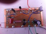
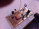
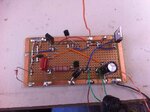
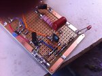
Ok, now the circuit works with no load, but when I put load, even 100mA, the NPN transistor gets very hot. I changed the BD137 for an 2N2221 to see if I could see any improvement, but nothing. There is a significant amount of current going through the NPN transistor, anybody have any idea what it could be? May the amplification?

15801507_1325733807448661_361387864_n.jpg15909611_1325734064115302_181062664_n.jpg15934669_1325734150781960_1250612721_n.jpg15941831_1325733930781982_648347200_n.jpg
 

It is reasonable to choose transistor control, because it is compatible with your 48V source. However I have played with this type in simulation and hardware, and it is easily prone to lapse into stagnancy, unless every little adjustment is right. You want to find the easiest thing that will nudge it back into oscillating.

* Gain needs to be high, so that a small change in output causes 'snap on-off action' in your transistors. (Your first schematic has a sziklai pair, which multiplies gain.)

* Bias needs to be tuned to a point where the circuit is not too stable in either state. On each side of that point you are trying to create the snap action.

* Since it is essential for the converter to oscillate continuously, install a monitor which tells you if it is, or whether it has stagnated.

I think I understand what you mean BradtheRad, you said about the Sziklai pair, but the MOSFET doesn't have a gain to multiply, in this case you suggest I use darlinton pairs in the NPN and PNP transistors to have a high gain?

And for the bias, what you think that can help to make the circuit less stable? I am pretty newbie to these type of circuits.

UPDATE: Do you think that the 1nF cap (C2 on E-Design's schematic) influence that stabilty? Maybe a higher capacitance one?
 
Last edited:

It is hard to see on your board if there is any mistake, unless you clean up the connections. You also have very long wires between components, which may give unwanted behavior due to parasitic inductance. Try to make the design a bit more compact with shorter connections. You want to minimize inductive loops in any switching regulator or power supply.

I will also suggest that you debug the design first at a lower (24 V) supply voltage, and only increase it if everything seems to function as expected.

Got it! Lower voltage and shorter connections. I will try and I post the results as soon as possible. Thank you very much.
 

It is hard to see on your board if there is any mistake, unless you clean up the connections. You also have very long wires between components, which may give unwanted behavior due to parasitic inductance. Try to make the design a bit more compact with shorter connections. You want to minimize inductive loops in any switching regulator or power supply.

I will also suggest that you debug the design first at a lower (24 V) supply voltage, and only increase it if everything seems to function as expected.

- - - Updated - - -

I will see when I have some time over the weekend to do a bit more analysis on this modified design. For now test with lower supply voltage.

- - - Updated - - -

Try it with the soft-start capacitor C4 (470 nF) disconnected and see if it makes a difference.

Thank you very much for the time you are spending helping me, and about the soft-start, I already tried without it. The first circuit that E-Design suggested (beggining of the thread) didn't had it. However, in this latest design suggested I already tried without the capacitor too. The 10nF capacitor in series with the 120 Ohms resistor makes some changes in the frequency of the circuit (at least in the simulation), that's why I tought it could change something.

As for the analysis of the real circuit, I will try to access some oscilloscope as fast as possible to check if the circuit is getting stagnated.
 

Shouldn't there be an input bypass capacitor?

I wonder if some amount of NPN transistor power dissipation is by design (non optimal bias).
 

Shouldn't there be an input bypass capacitor?

I wonder if some amount of NPN transistor power dissipation is by design (non optimal bias).

The bypass capacitor I admit I didn't tried. About the NPN transistor, it's getting extremely hot, about 2 seconds with a 0.5A load it gets impossible to put your hands on, for a transistor that should just switch the MOSFET, something is terribly wrong. If BradtheRad is right, maybe the stagnation of the circuit makes the current flow through the transistor.

IMPORTANT DETAIL: The voltage keeps regulated even with the NPN transistor getting hot, the circuit technically works, but the NPN is getting very hot, current is flowing through it somehow, but the switching keeps working.
 

Here is a simulation using the larger transistors. I added another zener diode (12 V) in series with the emitter of the NPN to prevent high current to flow through D7 and Q2 if the output is slow to come up to 12 V, as with start-up conditions or excessive load. Note that the original reference zener needs to be 24 V (or two 12 V zener diodes in series) as a result of this.

The peak and average power in the relevant devices are shown to be well within safe levels. The plots right next to the circuit show the transients during the first few mS after applying power.

There should be no reason that the NPN device should dissipate a lot of power now.

Simulation show a steady state efficiency around 90%.
Input power = 13.30 W
Output power= 11.85 W
 

Attachments

  • buck_48_comp1.png
    buck_48_comp1.png
    88.6 KB · Views: 184

Here is a simulation using the larger transistors. I added another zener diode (12 V) in series with the emitter of the NPN to prevent high current to flow through D7 and Q2 if the output is slow to come up to 12 V, as with start-up conditions or excessive load. Note that the original reference zener needs to be 24 V (or two 12 V zener diodes in series) as a result of this.

The peak and average power in the relevant devices are shown to be well within safe levels. The plots right next to the circuit show the transients during the first few mS after applying power.

There should be no reason that the NPN device should dissipate a lot of power now.

Simulation show a steady state efficiency around 90%.
Input power = 13.30 W
Output power= 11.85 W

Following E-Design's suggestion, I reduced the Vin to 24V, and it worked!!! The transistors are not getting hot, the MOSFET gets warm, since I got only 83% efficiency, not bad since I am using two slow transistors and I have the 100Ohm resistor between the collectors, which should compomise the switching speed (I guess?).

Another thing is that the inductor is doing that "piiiiiii" sound and the volume changes with the load resistance, so we know that now the circuit is oscillating. 24V OK, and since 48V doesn't make any sounds, I guess the circuit is not oscillating.

I tested the Zener diodes in series with de colletor and got the same hot NPN transistor as always, the input capacitor showed no results too. But since we noe know that probably the circuit is no oscillating, that should be the cause for all the problems, but the point is, how to make it oscillate?
 

Have you implemented all changes as per my last circuit? There are some differences with the circuit and values to operate with 48 V supply. Look carefully at value of R1 and connection point of R7.

The efficiency of this will improve slightly with higher loads due to a lower operating frequency. This can be seen from the load step response.
 

Attachments

  • Eff_load.png
    Eff_load.png
    71.5 KB · Views: 155
Status
Not open for further replies.

Similar threads

Part and Inventory Search

Welcome to EDABoard.com

Sponsor

Back
Top