Continue to Site

Welcome to EDAboard.com

Welcome to our site! EDAboard.com is an international Electronics Discussion Forum focused on EDA software, circuits, schematics, books, theory, papers, asic, pld, 8051, DSP, Network, RF, Analog Design, PCB, Service Manuals... and a whole lot more! To participate you need to register. Registration is free. Click here to register now.

[PIC] SPWM using PIC16F684

Status
Not open for further replies.

Hunain_Shuja

Junior Member level 1
Joined
Nov 10, 2016
Messages
16
Helped
0
Reputation
0
Reaction score
0
Trophy points
1
Visit site
Activity points
175
Hi,
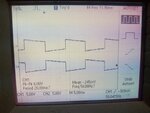
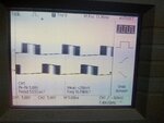
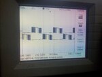
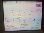
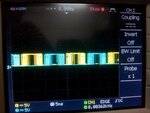
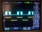
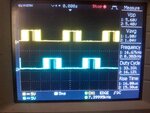
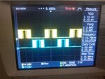
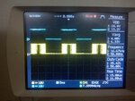
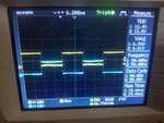
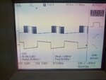
I'm generating SPWM using PIC16F684 microcontroller for inverter circuit . I followed Tahmid's blog and using his code to get SPWM output. I have simulated the design on Proteus i got the similar output as his, but when i build this design on hardware i didn't get similar output, i used the same steps as in proteus. The Spwm is not in proper shape . I'm attaching my results kindly tell me what is the issue in it?

.Using 16Mhz crystal with microcontroller
.5V DC Supply
.Taking output from pins 5,6,7,8

IMG_20161110_112901.jpgIMG_20161110_112935.jpgIMG_20161110_113010.jpgIMG_20161110_113530.jpg
 
Last edited:

Show us the circuit - preferably the schematic and a photo of how it has been built.
How are you measuring those signals (i.e. what wettings on the scope probe and the scope itself)? I can see the settings on the screen but (for example) are you using AC or DC on the probe?
In what way are the signals not the same? (I can see the AC coupling in the images you have shown but I don't know what you actually expect to see).
Susan
 
Hi,
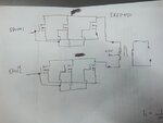
I attached the circuit diagram kindly see in this post .
I'm using Tektronix TDS1012 to see spwm output.
I'm not sure about this, but i think the probe is on Ac.
I'm talking about the shape of square wave.The horizontal edges of wave is not horizontal.I'm highlighting what is the mistakes in the above images? kindly see the attached images.
Screenshot_1.png Screenshot_2.jpg Screenshot_4.png
 

There comes out many questions, i think you should write your present situation briefly.

1. Did you setup your oscilloscope correctly according to your need?
2. Did you check your oscilloscope and probe are correct working?
3. Where did you find these types pulses in circuit.
4. where are The controller's pins (5,6,7,8) connecting.

I think you have connected your pins (5,6,7,8) to any circuit and that circuit is creating problem.
 

1)Yes
2)Yes
3)I have generated these pulses using PIC16f684 for my SPWM based Inverter.
4)I connect only microcontroller pins(5,6,7,8) to the oscilloscope, to check the output from MC.

Kindly check image, which i have attached in this post, i setup same configuration as in simulation .
Screenshot_1.png
 

HI,

* either your scope GND connetion is defective, --> use a good GND connection
* your scope probe is defective, --> change the scope probe
* or your scope channel setup is AC. --> set it to DC

you should send a photo of your circuit with the scope connections and a photo of your scope channel setup.

Klaus
 
@KlausST
Hi,
Alright I'll check all these things and i'll post all images tomorrow.
 

The problem is solved. My oscilloscope setting was on AC so i changed it to DC, by this i got my required output, here are the results.
IMG_20161112_114202.jpgIMG_20161112_115556.jpgIMG_20161112_120051.jpg

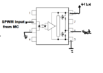
Now i gave these signals from the PIC16F684 microcontroller to Isolated Mosfet driver IC (TLP350) I got this results.
IMG_20161112_132746.jpgIMG_20161112_133124.jpgIMG_20161112_133527.jpg Screenshot_5.png

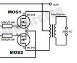
Now I'm moving to next step.I Don't want to use the H bridge configuration for my inverter. I'm using Push Pull topology for inverter design here is the configuration of Push Pull topology
Screenshot_3.png

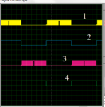
My question is which two signals should i use among these four signals to give it to the gate of MOSFETs.
Screenshot_4.png

I'm not sure. Signals (1 and 3) should be use. Signal 1 is input of MOS 1 and Signal 3 is input of MOS 2.

if i'm correct so is there a requirement of bootstrapping in this configuration .

I read somewhere that. In H bridge you have two sides one is high side and second one is low side. The high side is that when your load is connected to source of MOSFET and low side is that when load is connected to drain of MOSFET . We do bootstaring only on high side when using H Bridge.

So in Push pull topology the load is connected to drain , so I'm thinking there is no need of bootstrapping. I'm not sure.

Please try to answer all my these queries.
 

Attachments

  • Screenshot_3.png
    Screenshot_3.png
    58 KB · Views: 175
Last edited:
For Push Pull Circuit you need complementary PWM signals. You have generated Full_Bridge Signals. Only one Mosfet will be ON at a time. If you need more output power then you have to use more parallel Mosfets and also the transformer windings should be able to handle the higher currents.

You have to use 12-0-12V to 230V secondary transformer.

You are using bulky output transformer and hence you don't need High-side and low-side FET drivers. Your primary side voltage will be 12V and only half of the primary winding will be active at a time. You will be stepping 12V to 230V 50Hz AC.

Generate 1 SPWM signal and use a NOT gate to get its inverted signal. Feed PWM to one mosfet's gate and inverted signal to another mosfet's gate.
 
Last edited:

@Okada Thanks for the reply .

Will SPWM be the input gate signal for MOSFETs? OR simple PWM will be input signal for MOSFET. ( In push Pull circuit)

yes you are right the MOSFETs are in parallel in my design to increase the output power. I'm using three IRFP450 MOSFETs in parallel on half side of transformer and again three IRFP450 on other half side of transformer. kindly see below image.

Sorry for my drawing.
15095450_1055516024575955_2392556468882840801_n.jpg

Now i have dropped TLP350 Isolated MOSFET Driver due to its min Supply voltage(VCC) which is 15V and i want drive my MOSFETs at 12v,because i'm using a 12v battery .
see image below.
Capture.JPG

Now i'm using IR2100 gate driver IC which is perfect for my application min Supply voltage(VCC) 10v and it can drive two MOSFETS.
IR2110 - 6.png

But i have confusion here. A single output pin of IR 2100 driver can drive three MOSFETS which are connected in parallel on half side of transformer ? according to my push pull design.

IR2110 - 6.png

If i connect 2 more MOSFETs in parallel with Q1 ,(connect drain with drain, source with source and gate with gate) and connect gate with the pin 7 of IR2110 will IR2110 Drive all three MOSFETs without any error? same condition with Q2.

After this there is a requirement of Snubber RC circuit and LC filter and i have no idea how to choose the right value of (R and C) and (L and C) ?
 

Read this.

https://www.instructables.com/id/250-to-5000-watts-PWM-DCAC-220V-Power-Inverter/

For push pull you just need one PWM or SPWM and a complementary of PWM / SPWM obtained using 74HC04.

Only if you go for Half-Bridge or Full-Bridge topology you need FET drivers like IR21xx.

Are you using readily available bulky output transformer or are you getting it manufactured for your transformer specification ?

Read this regarding transformer design.

https://www.homemade-circuits.com/2012/02/how-to-design-your-own-inverter.html
 

@Okada Hi,

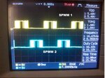
Now i got confused. I have generated Two SPWM signals from Microcontroller. SPWM 1 and SPWM 2 .
IMG_20161112_120051.jpg

This two signal are not complementary? Let suppose SPWM 1 is operating for 10ms (for positive half cycle of Sine Wave) while SPWM 2 is set to low (0v). Then SPWM 2 is operating(for negative half cycle of Sine Wave) then SPWM 1 is in low state (0v).

Isn't the same working principle just like in H Bridge there are two path to the flow of current, P1 is followed when Hi1 and lo2 are turned on while Hi2 and lo1 are off .
same condition for p2 when Hi2 and lo1 are turned on while Hi1 and lo2 are off.
brdge.gif

So in push pull topology there also two paths p1 and p2. when Q1 is on P1 will follow Q2 is kept off. or vice versa

Please tell me am i right or wrong?


I have design according to your suggestion used not gate IC. and the waveform looks like this.
Screenshot_1.png

----------

The reason why i'm using Gate driver is MOS IRFP450 requires gate voltage (10-15V) to fully turned on . The magnitude of SPWM output from Microcontroller is 5v.
i have connected practically Microcontroller with direct gate of MOS but MOSFET is not turning on . The reason is i want to step up 5V to (10-15v).


-----
Yes this transformer is the reason of all this confusion . I have old UPS which is not in use now, i'm using its transformer which is (12v-0 12v) to 220V and power rating is 500W.
I don't want to invest on transformer that's why i'm using this old transformer.
 

The signals are not correct. You have to generate 1 SPWM signals and get its complementary signal. Your Proteus signal shows 180 degree SPWM. You need 360 degree SPWM.

Use Logic Gate Power Mosfets N Channel with low Rds(on). eg: 3.8 m Ohms.

The signals shown in the oscilloscope (previous post) (not proteus signals) are correct. Thet are Half-Bridge or Push-Pull signlas for 180 degree SPWM. You can use those signals.

You have to configure MCU for Half_Bridge (Push-Pull) output and use P1A and P1B signals. No need to invert any signals.

I made a mistake in looking at the signals in post #8. Yes, you can use signals 1 and 3 shown in Proteus oscilloscope of post #8. Better generate Half-Bridge Outputs P1A and P1B and use it.

- - - Updated - - -

Show your CCP1CON register settings.


STE180NE10 will be the best mosfet for your application. You can use this for higher wattage inverter also. Mount this on heatsink and connect only gates to PCB. Connect Drain and Source using wires of proper guage using Ring Terminals screwed to Mosfet. Use a Fan to keep the mosfets and transformer cool.
 
Last edited:

@Okada thanks for the reply.

Can you please show me by picture , which type of waveform you are talking about ? Because i'm not getting this 180 and 360 degree part.

----

The signals shown in the oscilloscope (previous post) (not proteus signals) are correct. Thet are Half-Bridge or Push-Pull signlas for 180 degree SPWM. You can use those signals.
Are you talking about these signals ?
IMG_20161112_120051.jpg

-----

So signal 1 and 3 are SPWM signals.
-------

I'm Following Tahmid's blog for SPWM generation using pic16f684 and here is link .

https://tahmidmc.blogspot.com/2012/10/generation-of-sine-wave-using-spwm-in_10.html
 

The signals shown in post #14 is correct. you can use them but I am not sure about your FET driver circuit. Maybe it is correct but here a person has done it differently.

Each mosfet or mosfet bank will conduct for 180 degrees of sine wave and total 360 degrees is conducted by both mosfets.

https://microcontrollerslab.com/modified-sine-wave-inverter-using-pic-microcontroller/

Maybe he lacks the knowledge of using IR21xx devices.

- - - Updated - - -

These are some good Mosfets that you can use for the Inverter application.

STB80NF10
FDP8860
FDP8440
HUF75652G3

FDP8440 will be the best Mosfet. I just Ordered 10 of that.
 

@Okada

Thank you so much for the help its means a lot for a newbie just like me .

-------
I've read it and understand each and every part.
------
Thank you for the suggestion of MOSFET.

----

Now comes filtering part Can you guide me how Calculate the values for R and C in snubber circuit ?
and also for low pass filter L and C .
 

Isn't the same working principle just like in H Bridge there are two path to the flow of current, P1 is followed when Hi1 and lo2 are turned on while Hi2 and lo1 are off .
same condition for p2 when Hi2 and lo1 are turned on while Hi1 and lo2 are off.

View attachment 133622

This can be seen as: (1) a buck converter in one direction during one half of the cycle, then (2) a buck converter in the opposite direction during the second half of the cycle.

Your H-bridge must perform the switching action to achieve this.
 

What is your PWM frequency ? You need 50 Hz sine wave output and hence cut off frequency is 50 Hz.

There are bonline LC and Pi Filter Calculators. Try them. Lats say you get 60 uH and 2.2uF for the filter component values. L will be in series with the load and C in parallel.

Your load current for 500W inverter will be max

P = VI

I = P/V = 500W / 230V = 2.14A and so you have to use a 60 uH 3A or 4A inductor (ferrite core)

For C you will have to use a 400V or 450V type.
 
and also for low pass filter L and C .

The larger the Henry value, the more it 'chokes' AC. You'll need to experiment, to find a Henry value that is small enough to admit your desired Amperes at 50-60 Hz. Because if it is too large, it attenuates your output waveform.

Then find a C value which performs more filtering, and in addition you should look for power factor errors (because that is typical when you run AC through inductors). The capacitor has the role of correcting power factor. Its value should be carefully chosen, to be accurate.
 

@Okada

The SPWM frequency is 16kHz.

Is it the formula to calculate the value of L and C ? fc=1/(2*pi sqrt(LC)).

- - - Updated - - -

@BradtheRad Hi,

Before your post #19 i assumed the value for capacitor 10uf 450v and calculated the value of L using this formula fc=1/(2*pi sqrt(LC)). fc =50hz
then L=1H 5amp.

now i have to choose the smaller value for inductor so i assumed 1.5mH and by using above formula it give me C=4.5F. fc =50hz

if the above calculation is not correct then what value of L should i start ? and transformer also has inductance should i consider that too?
 

Status
Not open for further replies.

Similar threads

Part and Inventory Search

Welcome to EDABoard.com

Sponsor

Back
Top