Continue to Site

Welcome to EDAboard.com

Welcome to our site! EDAboard.com is an international Electronics Discussion Forum focused on EDA software, circuits, schematics, books, theory, papers, asic, pld, 8051, DSP, Network, RF, Analog Design, PCB, Service Manuals... and a whole lot more! To participate you need to register. Registration is free. Click here to register now.

[SOLVED] Why does this audio DAC need external filter inspite of having internal filtering?

Status
Not open for further replies.

matrixofdynamism

Advanced Member level 2
Joined
Apr 17, 2011
Messages
593
Helped
24
Reputation
48
Reaction score
23
Trophy points
1,298
Visit site
Activity points
7,681
The CS4334 is an Audio DAC. It already has internal on chip filtering and interpolation capabilities as clear from datasheet page 12 Figure 8. I assume that this means that no filter is require to remove the high frequency components that are typical of outputs on DACs. However, the recommended connection diagram on page 4 Figure 1 of the datasheet looks like this:
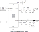
Untitled.png

Questions

(1) Why are there networks of resistors and capacitors at the output?

(2) Why is load shown as resistive, should it not be inductive as speakers are represented? If a power amplifier is being used at the output than this makes sense.

(3) Why is there in arrow pointed to right after the RL as if the signal goes beyond the RL?

(3) Why is C dependant on the load? Certainly if we want to get a specific frequency response, we should have fixed values for RC in the high and low pass filters.
 

Hi,

I recommend to read fome documents about digital audio processing includinc the theory of audiao ADCs, DACs, anti-aliasing-filters and reconstruction filters.

1) Two problems: You need a reconstruction filter. It can be partly made with digital filters, but you need analog filters, too. Here you see a 3u3 capacitor. This is way too big to include on a semiconductor chip.

2) The output doesn´t go to a speaker directely. It goes to an amplifer.
Btw: speakers are by far not always inductive. Many speakers have an inductive coil inside, yes, but each speaker has a membrane and this moving mass acts like a capacitance. And for sure there are real (resistive) parts. They generate the audible power (and the permissive heat). A speaker is a complex system and the impedance is complex, too. At one frequency it may be capactive at another frequency it may be inductive (always with resistive components).

3) This RL is either included in the amplifier´s input resistance (impedance) and/or you need to add one. With this resistor you can calculate the value for "C" (the formula is nearby). Without knowing "RL" you get not calculable resonances and not flat passband.

4) see 3. (here I recomend to read about passive R-L-C filters and filter characteristics like: passband ripple, stop band attenuation, phase shift...)

Klaus
 

I presume you understand that most of the filtering of this Delta-Sigma DAC is done in the digital domain by an oversdampling digital filter.

According to datasheet, I would assume that the output filter is not required because the DAC already includes an analog output filter to remove sampling residuals.

There's no specification or further description of the low-pass filter in the "recommended connection diagram". It's purposed is mentioned in datasheet section 3.1:

The digital interpolation filter increases the sample rate, Fs, by a factor of 4 and is followed by a 32× digital sample-and-hold (16× in HRM). This filter eliminates images of the baseband audio signal which exist at multiples of the input sample rate. The resulting frequency spectrum has images of the input signal at multiples of 4 Fs. These images are easily removed by the on-chip analog low-pass filter and a simple external analog filter.

The filter dimensioning is for a fixed cut-off frequency Fs/2. The circuit details don't look particularly meaningful to me.

- - - Updated - - -

It should be noted that a first-order low-pass at Fs/2 considerably changes the overall frequency characteristic of the DAC, thus I wonder if it's well considered.
 
Hi,

The output of the DAC is still digital somehow. It is not smooth like analog it is still in steps. Tiny steps.

These small steps carry high frequency residuals. You don´t want this. And a folowing analog amplifier may have problems with high dU/dt (although small steps).
Therefore one tries to suppress these steps. A part of this is done inside the IC.

***
To the datasheet:
it says:
4.7 Analog Output and Filtering
The analog filter present in the CS4334 family is a switched-capacitor filter followed by a continuous time
low pass filter. Its response, combined with that of the digital interpolator, is given in Figures 15 - 22.

When you look at the response in fig. 15 then you see the HF is suppressed by 50dB only. Too bad for a high fidelity audio signal.
(Switched capacitor filter is relatively noisy, but it´s benefit that it self-adjusts with sampling frequency.)
Additionally there may be noise between internal GND and external GND (ground bounce). This can not be filtered inside the IC, it needs to be filtered externally.

***
And there is the 3u3 high pass filter...
The internal circuitry works with single supply, positive only. The analog output signal is biased (maybe to VCC/2).
But an audio signal is considered to be positive and negative.
The 3u3 capacitor removes the DC bias.

Klaus
 
OK, I understand. I was misled by the diagram Figure 8, the heading "Analog low pass filter" and these words:
3.4 Analog Low-Pass Filter
The final signal stage consists of a continuous-time low-pass filter which serves to smooth the output and
attenuate out-of-band noise

But as you have pointed out, later it does mention that:
4.7 Analog Output and Filtering
The analog filter present in the CS4334 family is a switched-capacitor filter followed by a continuous time
low pass filter. Its response, combined with that of the digital interpolator, is given in Figures 15 - 22.

Is this really not a contradiction? :shock: Switched capacitor filter is a discrete time filter rather than a continuous time filter!

How folly of me. Anyway, since it is clear that the output is infact having high frequency transients due to the switched capacitor filter, I only need to know these things:
(1) Is it technically correct to call switched capacitor filter as analogue? Isn't it altleast half-truth?
(2) Since the DAC itself cannot drive a speaker load which is very low impedance, the DAC shall interface with an audio amplifier via the passive filter shown in the original question. How does one find out what the RL value shall be under these circumstances?
 

Hi,

1) Read the datasheet thouroughly: There is a switched capacitor filter AND an analog filter inside the IC.

2) as long as your amplifier´s input impedance is well above the 560 Ohms it is not critical. But some have lower impedance or you add some extra resistor, then you have to take care about it.

(Test load RL is given with 10k Ohms. You should not load it with less than 3k Ohms)

Btw: It´s easy to do your own search "load" within the datasheet as PDF.

Klaus
 

Thanks for demystifying this DAC :)

One last question, what is the purpose of the 10kohm 560ohm potential divider? I assume it is to reduce the output volume since if the maximum output voltage is applied by the DAC output, it shall create very loud sound from the amplifier. However, I assume that the same effect can be achieved by using a potential divider at the amplifier output, may be implemented using a variable resistor for volume control.
 

Hi,

the 10k is just an "simulation" of a usual audia amplifier input.
The is needed to perform an R-C low pass filter. Without a series resistor it is impossible.

It is not used to attenuate the sound level. Use a pot for volume level adjust...if you use a 10k pot then this is exactely the load to your DAC output.

Klaus
 
Switched capacitor filters are considered analog, they use OP's, analog switches and process analog signals. They are amplitude continuous but time discrete. Digital filters are both amplitude and time discrete.

Due to the time discrete signal processing, switched capacitor filters share some design methods with digital filters, e.g. z-domain analysis.
 
OK, I understand that while switched capacitor filters are discrete time and some tools used to analyse digital circuits can be used with them, they are not considered digital. This is clear. The low pass high pass filter reason is clear.

It is obvious that the 3.3u Capacitor and the 10k resistor form a high pass filter. Similarly the 560ohm resistor and C form a low pass filter.
Q: But, what is the function of the 267kohm resistor that directly shunts the output to the ground?
Does this have something to do with preventing pop sounds in the audio? Current to voltage conversion? Some sort of impedance matching?

- - - Updated - - -

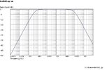
Assuming RL=10kohm, I get C=3.4nF from the formula. Using these values I have used the awesome **broken link removed** to generate the bode plot, the frequency respons looks like this:

Untitled.jpg

- - - Updated - - -

KlasST said about RL "Without knowing "RL" you get not calculable resonances and not flat passband.". However, as far as I am aware, for resonance we need to have inductive component together with resistive to make a 2nd order system. That is not the case here. The frequency response curve also looks quite flat in the passband. Therefore, it not clear what was meant by the original comment as the wording appears jumbled.
 

Hi,

I admit that my description lacks of information. I had a picture in mind: The DAC and then an audio amplifier.. connected with shielded audio wires. The wiring, the connectors and the amplifier input build a complex load. Surely with inductive components. Therefore every resistor in this chain helps to reduce resonances.

But I agree, if you keep on the given schematic, there are no inductances, and thus you will not see any resonances an a simulation.

Klaus
 
OK.

If someone asks why a specific value of 267kohm (which is quite big), how would you answer?
 

Internal filtering is probably just for glitch energy. The
external would be set up to remove anything that falls
outside the audio range; if it's an audio application then
you have no use, only waste power and maybe get ugly
intermodulation, from sample-step harmonics and so on.

As to RL specific value, somebody had to put something
on the app note and maybe they just made it up. Making
the capacitors return to zero is good hygiene (might not
want them charged up while the part is still down, or in
the process of powering up). Arbitrary values commonly
get put and if they don't cause a problem, stick around.
 

If someone asks why a specific value of 267kohm (which is quite big), how would you answer?
I already gave an answer in post #3
The circuit details don't look particularly meaningful to me.
Please notice that the datasheet Analog Characteristics are referring to simplified Figure 2 rather than Figure 1 schematic. Which can be read like, the "recommended connection" is not required to achieve the specified behavior, but has been considered somehow useful, without further explanation.

I agree with dick_freebird that the DC load resistor's purpose might be to discharge the coupling capacitor when the circuit is unpowered, possibly reducing power-up transients. But that's just a guess. If it's right, I still won't think too much about the specific resistor value.

As said, I'm generally skeptical against the application circuit because the low-pass filter contradicts the intended overall frequency characteristic. It's not unusual to have low-passes here and there in an audio signal chain, but you won't place it particularly in a DAC application circuit promising 0.1 dB pass band flatness.
 

Hi,

As said, I'm generally skeptical against the application circuit because the low-pass filter contradicts the intended overall frequency characteristic. It's not unusual to have low-passes here and there in an audio signal chain, but you won't place it particularly in a DAC application circuit promising 0.1 dB pass band flatness.

I´ve seen sophisticated audio equipment with analog and digital filters where only the combination of both results in the flat frequency response.
I doubt that this is the case here, because the analog filter is too close at the frequency of interest, that capacitor and resistor tolerances affect the specified flatness.

I´m skeptical, too.

Klaus
 

The datasheet says that the combination of digital filter and internal analog filter achieves the specified frequency response. Adding a second first order low-pass changes this optimized frequency characteristic.

But I made a mistake. The external filter cut-off is 2FS rather than FS/2. The magnitude drop at 20 kHz is only 0.18 dB then (for 48 kHz FS). So the recommended circuit is O.K. in this regard.
 

Status
Not open for further replies.

Similar threads

Part and Inventory Search

Welcome to EDABoard.com

Sponsor

Back
Top