Continue to Site

Welcome to EDAboard.com

Welcome to our site! EDAboard.com is an international Electronics Discussion Forum focused on EDA software, circuits, schematics, books, theory, papers, asic, pld, 8051, DSP, Network, RF, Analog Design, PCB, Service Manuals... and a whole lot more! To participate you need to register. Registration is free. Click here to register now.

[SOLVED] P10 led connection explanation

Status
Not open for further replies.

thannara123

Advanced Member level 5
Joined
Jan 7, 2010
Messages
1,602
Helped
122
Reputation
244
Reaction score
116
Trophy points
1,353
Visit site
Activity points
10,640
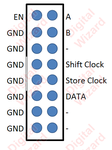
I bought a p10 led module

p10_display_32x16_red_back.jpg

p10_display_pinout.png

I had interfaced with pic ,8051 avr earlier with myown (made by me) led matrix .
No I want to interface it with p10 led module .And I bought it .The above pins are shown . what i s A and B in . how to understand it .
I have added a ot of matrix in my program for cascading the matrix . what about the programming in p10 LED .
 

I think they use 74HC595 shift registers, so these connections present to connector is of the shift register IC.
Can you tell, from where you buy these P10 Cards. I asked because you are from India and i would like to buy these cards also.
 

what is A and B ?
i purchased it from http://store.extremeelectronics.co.in/P10-32x16-LED-Display-Matrix-RED.html

- - - Updated - - -

Anyone has its datasheet ?

- - - Updated - - -

only give the raw data where can i give the column data

Thanks for the store information.

You can have a look at this link.
http://digital-wizard.net/avr_projects/p10_led_display_panel_interface

For Line A and B, i am not sure, but they are used to control the Upper and Lower 8 rows.
As 74HC595 IC is a 8-bit shift register, so to Handle a display of 16x32, two shift registers are used, one will control the upper 8 rows and another will control the lower 8 rows.

But i am not sure.
 
AB is 2 to 8 line decoder signal ? right ?

- - - Updated - - -

What changes are to made in the following program to interface p10 led module instead of 8x8 led matrix

Code:
#include <REGX51.H>
#include<delay.h>
sbit DS  = P1^6;   // Loading parallel data to HC165.
sbit SH_CP = P1^4;
sbit ST_CP = P1^5;


void sendserial(unsigned char);
unsigned char temp;
unsigned char a[]= { 0xFF, 0x88, 0x8C, 0x8A, 0x71, 0x00,
                     0x7E, 0x81, 0x81, 0x81, 0x7E,0x00,
					 0x7E, 0x81, 0x81, 0x81, 0x7E,0x00,
					 0xFF, 0x40, 0x30, 0x40, 0xFF, 0x00,
					 0x28,0x28,0x00,0x00,0x00,0x00,0x00,0x00,0x00
					  };
void scroll_data(void);

unsigned int i2,l,i,j,k=32;
void main()
{

  while(1)
   	scroll_data();


  	 }


void sendserial(unsigned char Serial_data)
{  unsigned char compare_data ; 
       		
  
    for (compare_data = 0x80; compare_data; compare_data>>=1)
      {
	      
        if (Serial_data&compare_data)
            DS = 1; // Data 1	
        else
            DS = 0; // Data 0 
		
		 SH_CP = 0;
	     SH_CP = 1; 
		  							         
      }
	  
} 

 void scroll_data(void)
 {
 
 
            for (i2=0; i2<4; i2++)
	         {
	          for(i=0; i<7;i++)
	   {	
	    P3=(1<<i);
	      sendserial(~a[i]);
		 sendserial(~a[i+7]);  
		 sendserial(~a[i+15]);
		
	      ST_CP = 0;
	      ST_CP = 1;	
		  
		 delay(5);
		 }
		 
	  	}
     
	 
	 temp= a[0];
            for(j=0; j<k; j++) 
			 {
			 a[j] = a[j+1];
			     if(j==k-1)
			     {
				  a[j] = temp;
				  }
			  }	 
	
	}

Capture.PNG
 

It is straighfoward deduce that the first thing to do is to increase the size of variables temp and a[], and corresponding code which handles them in order to reach the just added extra bits.
 

earlier the forum was highly helpful

Perhaps because now the forum ( members ) are not motivated to help anymore the ones who do not clearly evince a previous research, an initial guessing, or even an attempt to start making themselves something before asking for a solution.
 
I don't know how you got "the correct answer" from a link that apparently uses a completely different interface and mux scheme.
 

I don't know how you got "the correct answer" from a link that apparently uses a completely different interface and mux scheme.

A and B is there used to RUN /Scan the rows with a decoder ?
 

A and B is there used to RUN /Scan the rows with a decoder ?

Isn't that information available at the link "Download P10 Datasheet in PDF" that is currently present at the seller link you provided above ? I noticed that for downloading it we first should to subscribe there, but I'm too lazy to do that right now, and I sincerely hope that this was not the reason for which you didn't as well.
 

earlier the forum was highly helpful ..

We are all interested in helping others but it does not mean that we shall do your work of learning. You are expected to gain knowledge sufficiently so that you can understand and learn the basics.

We help you to learn the basic principles and if you have some queries, we explain. But it should not be like that we give you a schematic and you do the soldering.
 

Perhaps because now the forum ( members ) are not motivated to help anymore the ones who do not clearly evince a previous research, an initial guessing, or even an attempt to start making themselves something before asking for a solution.
Sir i searched that above 5 hours more .. i didnt seen that datasheet thank you very much helped ...
 

Status
Not open for further replies.

Part and Inventory Search

Welcome to EDABoard.com

Sponsor

Back
Top