Continue to Site

Welcome to EDAboard.com

Welcome to our site! EDAboard.com is an international Electronics Discussion Forum focused on EDA software, circuits, schematics, books, theory, papers, asic, pld, 8051, DSP, Network, RF, Analog Design, PCB, Service Manuals... and a whole lot more! To participate you need to register. Registration is free. Click here to register now.

[SOLVED] Trying to control an AD5142 potentiometer with an Arduino

Status
Not open for further replies.

DigitalDeath

Junior Member level 1
Joined
Jun 30, 2016
Messages
18
Helped
2
Reputation
4
Reaction score
2
Trophy points
3
Visit site
Activity points
169
Hello everyone,

This AD5142 IC has me stumped. I have tried every combination I can come up with and there is nothing I can do to make it work.
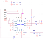
Here's the schematic:
AD5142_SCHEMATIC.PNG

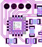
Here's the actual layout with the programming probe pads with the corresponding microcontroller controller terminals:
AD5142_LAYOUT.PNG


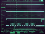
Here are the signals being sent for writting a 1 to pot 0:
AD5142_LOGICANALYZER.PNG

I have tried floating -INDEP, connecting to to ground and to +5V. I have tried all 4 modes of SPI_MODE0 to SPI_MODE3

Here's a sample of a simple program I've tried:

Code:
#include <SPI.h>
void setup() {
  
  // pin 10 is the slave select for the digital pot
  pinMode( SS, OUTPUT); // set the slaveSelectPin as an output
  digitalWrite(SS, HIGH); // take the SS pin high to de-select the chip
  
  // MISO input needs to be ;ulled up for the AD5142
  pinMode( MISO, INPUT_PULLUP);
  
  SPI.begin();  // initialize SPI
  
  // set SPI speed to 500 kHertz, MSB, NORMAL LOW CLK and FALLING EDGE
  SPI.beginTransaction (SPISettings (500000, MSBFIRST, SPI_MODE1));

  // make sure the control register is correct:
  digitalWrite(SS, LOW);// take the SS pin low to select the chip
  SPI.transfer(0b11010000); // Copy serial register data to control register command 16
  SPI.transfer(0b00000011); // D2= 0 = potentiometer mode, D1=1 = enables EEPROM programing, D0=1 = allow update of wiper position
  digitalWrite(SS, HIGH); // take the SS pin high to de-select the chip

}

void loop() {
  writeOne();
  delay(10);
}

void writeOne(){
  
  digitalWrite(SS, LOW);// take the SS pin low to select the chip
  
  SPI.transfer(0b00010000); // command 1= set pot, pot selected= 0
  SPI.transfer(0b00000001); // pot value= 1
  
  digitalWrite(SS, HIGH); // take the SS pin high to de-select the chip

}


This code on SPI mode 0 works perfectly fine on an AD5204 that used raising edge clock from the same family.
Here's a link to the 5142 Datasheet.

And here's the pinout:
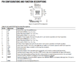
AD5142_PINOUT.PNG

When turned on the wiper starts in the middle of the pot range as expected by default from factory but I can't get it to respond in any way.
I made a circuit with only the IC and no luck, I even soldered small wires to each pin to the IC by itself to make sure the connections were correct but no luck.

I tried the code with another IC from the same family and it worked perfectly fine.
This code on SPI mode 0 works fine on an AD5204 that uses raising edge clock from the same family.

I know it'll be some tiny little detail I forgot or missed that will make it work but I'm stumped right now.

Any help will be appreciated.
 

Hi,

I can't see how the IC is supplied with GND signal.

Klaus
 

Yes its grounded with vias to the ground plane layer in the square center pad. If you look at the layout its marked GND in pink. I just didnt activate the vias visibikity for the pic.
 

Hi,

If you look at the layout its marked GND in pink.
Yes, but "marking" is no physical connection. ;-)
And the vias are not visible to us...

Klaus
 

Yes but the vias are there and the center square pad as well as the pins connected to the pad are grounded. If I turned the via visibility you wouldn't be able to read the pin names.

That being said lets not get off topic. I need help with figuring out why this particular IC is not responding to any command that's sent to it. This code with the correct polarity and phase works with other pots from the same family. I'm missing something but I can't figure out what.
 

Hi,

try to READ back the programmed value
* Does the device respond at all?
* does it return the default values or the programmed value?

***
Please give a detailed error description:
but I can't get it to respond in any way
... says nothing

How exactely did you measure, what did you expect, what happens instead?
(Measurement device, measurement points, values)

Klaus
 

If you look at the circuit there's a 2k resistor connected to the top of the pots and to 5V. The other side of the pots are connected to ground.
When the device powers up it loads 80h by default from factory so the wiper is in the middle of the travel and I get 5 * 5/(10+2) or about 2V at the wiper. Nothing I send to the IC changes that voltage.

I also monitor the MISO line with a scope and it remains pulled up high when I try to read via SPI commands so I get 255 as a result from a read RDAC command via SPI. To test the protocol I manually short the MISO line to ground and the SPI returns 0 as expected so the arduino SPI side seems to be working.

Keep in mind two things.
1. I have the same program working on an AD5204 using the rising edge clock that the AD5204 needs.
2. I tried connecting an IC by itself in the air with small wires soldered to the pins and ground pad with no pc board jut to make sure visually it's correctly connected and still doesn't work.

Here's a pic of an earlier version of the board's ic footprint so you can see what the grounding vias look like:
image.jpeg
 

I tried the code with another IC from the same family and it worked perfectly fine.
This code on SPI mode 0 works fine on an AD5204 that uses raising edge clock from the same family.

You must be aware that both ICs have slightly different serial control words, and so the code should not be exactly the same. In the AD5204 the frame format is
A[2-0]D[7-0]
whereas in the AD5142 the frame format is
C[3-0]A[3-0]D[7-0]
 

Yes I'm aware of that. If you see the code I posted above it says
Code:
SPI.transfer(0b00010000); // command 1= set pot, pot selected= 0
  SPI.transfer(0b00000001); // pot value= 1

where the command C[3-0] is 0001 (write to the RDAC), the pot selected A[3-0] is 0000, then the data D[7-0] sent is 00000001
You can also see in the posted that the SPI pulses correspond to those values.
 

I'm not sure if you can do by splitting this way, anyway, considering that the size of control word of the AD5142 is exactly 16 bits, I would recommend you try using the transfer16() function instead.
 

I did that too it makes no difference. As a matter of fact as long as the CS is not raised there is no difference in what the IC sees either way.
 

Hi,

Reading your latest post I now assume a bad solder joint...maybe in the cs line...

Klaus
 

I think you misunderstood what I wrote. I meant that as per the protocol it makes no difference that the clock pulses are 8+8 or 16 as long as the CS line is not raised the SPI takes the pulses both ways.
 

Mystery solved.
Bought an evaluation kit for the part.
The evaluation kit's daughter-board worked with the PC software and the logic analyzer's SPI waveforms and timing were identical to the ones coming from the my Arduino so I unplugged the daughter-board from the motherboard and connected the pins to the Arduino and it worked on the first try.
Turned out I wasn't doing anything wrong, it was just bad parts.:???:
That's 6 parts from a cut-tape that were defective. First time this ever happens to me.
Had to throw them out so I wouldn't use them by mistake and ordered more form a different supplier.

I guess the only good thing about this is that this thread now works as a tutorial for controlling the AD5142 with and Arduino UNO via SPI.
 
Status
Not open for further replies.

Similar threads

Part and Inventory Search

Welcome to EDABoard.com

Sponsor

Back
Top