Continue to Site

Welcome to EDAboard.com

Welcome to our site! EDAboard.com is an international Electronics Discussion Forum focused on EDA software, circuits, schematics, books, theory, papers, asic, pld, 8051, DSP, Network, RF, Analog Design, PCB, Service Manuals... and a whole lot more! To participate you need to register. Registration is free. Click here to register now.

boost output current of IR2184

Status
Not open for further replies.

Electro nS

Full Member level 6
Full Member level 6
Joined
Mar 9, 2013
Messages
324
Helped
49
Reputation
98
Reaction score
48
Trophy points
1,308
Activity points
3,818
I am using the IR21844 in half bridge configuration , now i have to modify the circuit for a larger mosfet (2500nC gate charge total) , i would like to boost the output current into 4-5A ( from the original 1.4A) and keeping the same Driver since i donot want to change the logic side of the circuit.

IR mensions this in one of its appnote :
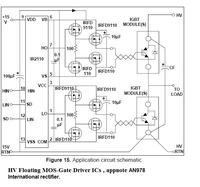


I would like to know if this circuit ( the 2 cascade totem poles ?) can be simplified more or replaced by IC that boosts the current.
 

I am using the IR21844 in half bridge configuration , now i have to modify the circuit for a larger mosfet (2500nC gate charge total) , i would like to boost the output current into 4-5A ( from the original 1.4A) and keeping the same Driver since i donot want to change the logic side of the circuit.

IR mensions this in one of its appnote :


I would like to know if this circuit ( the 2 cascade totem poles ?) can be simplified more or replaced by IC that boosts the curren

Hi
I highly recommend you to replace your driver for this aim . because , bootstrap drivers need to be connected into the Both H and L side directly to work properly .
Are you familiar how bootstrap drivers are working ?

Best Wishes
Goldsmith
 
I highly recommend you to replace your driver for this aim . because , bootstrap drivers need to be connected into the Both H and L side directly to work properly .
Are you familiar how bootstrap drivers are working ?
The necessary connection between driver and output stage for the VS and COM nodes are made through the twisted gate driver lines. I agree with goldsmith that the connection is probably not direct enough to work properly. You might e.g. observe undershoot of the VS node which can easily kill the bootstrap driver. Changing to a true isolated driver is strongly suggested. Many IGBTs require also bipolar gate drive for switching performance and shoot-trough prevention.

Boosting bootstrap driver to 5 or 10 A as such can be achieved with complementary bipolar voltage followers. I fear the sketched common source MOSFET buffer would suffer from high transverse current (driver internal shoot through).
 
i totally understand bootstrap gate drivers and i have worked with IR21844 and it is a wonderful IC , espically the logic part of the circuit , the only limitation i am facing is the output current . I am now convinced that using complementary npn pnp (in emiiter follower or totem pole might be the solution)
my switching frequency is 20Khz , i donot know if this will cause limitation in BJT driver ??
and i also decided to place the driver on the top of the power module , so the distance from gate and source to driver is less than 5cm .
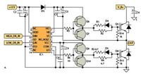
the circuit will be something like this :

please can you sugest npn and pnp discrete or a matched pair in one IC that is suitable in such application , i am not familiar with BJT charactaristic curve , and i donot know how to choose wisely for speed and gain
 

20 kHz isn't actually fast. An important point is choosing transistors with sufficient current gain at higher currents. Zetex/Diodes has a series of complementary SOT23 transistors (ZXTN2013, ZXTP2025) for up to 5 A continuous current that are often used for gate drivers, for higher currents complementary medium current audio transistors can be used.
 
thank u very much !

i have also found app note from diodes zetex for this application :**broken link removed**
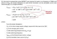
in page 2 the calculations for the power loss

i get that the right part is negligable , but shouldnot the left part be P = Q*f*I right ?? , why is he using (Vcc-vgs/2)*Q*f , and by the way vgs should be = vcc right ? which is 15v. he used vgs=8v.

hopefully SOT23 package will be able to dissipate around 0.7w to 1w
 

I wonder how you arrive at several 100 mW with only 20 kHz switching frequency. That's unlikely with medium size IGBT.
 

I wonder how you arrive at several 100 mW with only 20 kHz switching frequency. That's unlikely with medium size IGBT.

total gate charge : 2500nC , Vcc =15v , turn on speed required : 1% 20khz = 0.5us

then I=Q/t= 2500nC/0.5us=5A .

this last equation i am not sure about and i would like you to correct my calculation
P=Q*f*I=2500nC * 20000hz * 5A = 0.25 w , or if P=Q*f*V=2500nC*20000hz*15v=0.74w
donot know which is correct !!!
 

Your equation is wrong. P = Q*f*V would be correct (As*1/s*V = W). So yes, if the gate charge is in the range of several µC, you get W driver power with 20 kHz switching frequency.

A problem is that IGBT modules with µC range gate charge are usually expecting bipolar gate drive, so they won't work well with basic IR21xx driving. I see that the IRF application note has also a bipolar variant with auxiliary negative supply, I guess that's why they introduced the double inverting MOSFET buffer shown in post #1. It seems to be like overstretching the reasonable application range of bootstrap driver technology. A somehow obsessive "yes we can large IGBTs" application engineer's claim.
 
It seems to be like overstretching the reasonable application range of bootstrap driver technology. A somehow obsessive "yes we can large IGBTs" application engineer's claim.

The same can be said for large mosfet module ?
 

Status
Not open for further replies.

Similar threads

Part and Inventory Search

Welcome to EDABoard.com

Sponsor

Back
Top