Continue to Site

Welcome to EDAboard.com

Welcome to our site! EDAboard.com is an international Electronics Discussion Forum focused on EDA software, circuits, schematics, books, theory, papers, asic, pld, 8051, DSP, Network, RF, Analog Design, PCB, Service Manuals... and a whole lot more! To participate you need to register. Registration is free. Click here to register now.

2sc1627 and GND problems

Status
Not open for further replies.

Allachikatillo

Newbie level 5
Newbie level 5
Joined
Jan 13, 2016
Messages
9
Helped
0
Reputation
0
Reaction score
0
Trophy points
1
Visit site
Activity points
71
Hi!

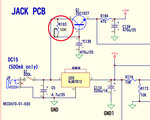
I'm trying to clone vestax from original circuit for my study project. Made the PCBs, but it doesn't work properly. The volume is low, pots doesn't much effect the sound (completely turned down pots still sending signal) and phones doesn't work as well. Removing H7C connection, totally removing U7 from the socket or that transistor 2sc1627 do nothing. Capacitor polarity is right. Shorting out the C and E of the 2sc1627 makes U19 working, but U7 distort the sound in phones. It would suggest that the fault is in that part of the circuit causing it to draw too much current. Its about 1,2V on the E, C is 15V measured to ground, B to E is 9V, E to C is 14V. No matter with or without "To Phones" load connection. U7 V+ pin is 1,2 V. Every Cap is wright oriented, and PCBs is without solder bridges.
I've checked the pcb and everything is connected right.

The solving this problem doesn't mean the solving problem of the whole circuit. The question is why the original circuit doesn't work as it should be. Changing the transistor or supply part doesn't solve the problem with pots (i use this https://lib.chipdip.ru/995/DOC000995779.pdf, every pot is well grounded). I think something is causing all this problems, but can't find it.

I surmise thats its all about GND or supply in general. I have 2 PCBs with separated ground planes with single point ground connection for GND, GND1 and GND3 (the second PCB).

Maybe I misread the schematic and make a mistake with layout? What should I check or re-check, to find the problem?

- - - Updated - - -

UPD: Strange thing happen - if i totally disconnect GND2 point on H2C/CN2J the LED11 (Power Led) is still working (while the pwr is on). How it can be explained, there is no any GND connection on this board.
 

Attachments

  • PCV-0021.pdf
    800.5 KB · Views: 214

Looks like some sort of grounding problem but I can't understand why you think the power LED would be affected by removing H2C ground as that only disconnects the U19 output stage. The LED is powered between the 12V output of U20 and the power source ground so it should be lit whenever power is present at the input socket.

Brian.
 

Hi, Brian. There are two pcbs with separated grounds, with single poin connection on H2C/CN2J. It cannot run off just a positive supply. I check the pcb for a short-out but there is no any.
 

I assume the two PCBs are the one outlined in red and the one outlined in blue.

I can't see any connectors carrying the ground between them. The 'line with diagonal feet' grounds and the 'triangle' grounds must be connected together somewhere for it to work properly. I suggest using a testmeter to check the resistance between the various gound points to check they are all joined together.

The LED is effectively connected across the output of the 12V regulator U20 so it should not change if H2C ground is removed.

Check from the power socket ground to H4C, you should see these voltages:
Pin 1 = 12V
Pin 2 = 6V
Pin 3 = 6V

then check the voltage across C132, it should be about 14V.

Brian.
 

Correct, two pcbs outlined in red and blue. Two grounds are connected together in one point at H2C (pin2). Thats why I wonder why the LED11 is still working without "pin2" connection.

I check continuity of the gnd signal all over the ground plane, and everything is ok.

The voltage for Vcc, both of 1/2 and across C132 is as you write it.

How do think, what's the problem with it?
 

The base to emitter voltage of the 2SC1627 is 9V but it is supposed to be about 0.7V. I think you have its B and E pins swapped. Its datasheet shows the collector pin is in the middle so simply turn the transistor around.
EDIT: Replace the transistor because you might have overheated its fragile base-emitter junction and install the new one with the correct pins.
 
Last edited:

The base to emitter voltage of the 2SC1627 is 9V but it is supposed to be about 0.7V. I think you have its B and E pins swapped. Its datasheet shows the collector pin is in the middle so simply turn the transistor around.
EDIT: Replace the transistor because you might have overheated its fragile base-emitter junction and install the new one with the correct pins.

Audioguru,

Thats the first thing I've checked. And the second was the replacement of the 1627. So it's ok about it. The problem is not there.
 

I find it strange that you stll hear output when the controls are all turned to minimum.

Can you try this please:
Using headphones, confirm that a signal fed to the right input is only heard in the right earphone and a signal fed to the left input is only heard in the left earphone.

I'n trying to work out if there is a common point between the channels that is cross coupling instead of gounding.

Brian.
 

The problem is that the base-emitter voltage of the 2SC1627 is much too high so it is burnt out. Its base voltage should rise slowly when power is applied as C138 is charged by R193.
Maybe the 2SC1627 is overloaded by C132 having backwards polarity?

EDIT: How can the emitter of the 2SC1627 be correct at +14V and only +1.2V at the same time??
 
Last edited:

See reply in post #5. The 2SC1627 must be operating if it is only dropping Vbe and a little in the series resistor. The voltage at it's output is already confrmed to be correct by measuring across C132.

Brian.
 

See reply in post #5. The 2SC1627 must be operating if it is only dropping Vbe and a little in the series resistor. The voltage at it's output is already confrmed to be correct by measuring across C132.

Brian.

Then I guess the first post about it is wrong.
 

I find it strange that you stll hear output when the controls are all turned to minimum.

Can you try this please:
Using headphones, confirm that a signal fed to the right input is only heard in the right earphone and a signal fed to the left input is only heard in the left earphone.

I'n trying to work out if there is a common point between the channels that is cross coupling instead of gounding.

Brian.

Hm, I hear only the output (even the U19 is off) - left on the left, right on the right, but not the monitor output.
I have to short out the C and E to start it work - so it distort left channel on the left, right on the right :)

- - - Updated - - -

Is it correct that 9v base-emitter reading could mean the transistor is shorted ('cos it should read about 0.7v)? I can't find out if excessive load has damaged the transistor.

For the life of me I can't understand one thing the reason why Led11 run off just a positive supply (without only one negative V supply on H2C/CN2J). It loads LED11 about 1.5V without H2C/CN2J (pin2) connection.
 

It seems odd to me that the LED current isn't returned to the same PCB that provides it but a few mA wouldn't upset its working. The current probably flows to the 'blue' PCB ground then by various leakage paths to a lower voltage. With 12V at it's anode it only need to connect a point of about 10V or lower for it to light up.

It does seem that the voltage across C132 is wrong. It comes from the emitter of the 2SC1627 which is why shorting C and E makes the voltage rise. All the 2SC1627 does is provide a slow rise in supply voltage so you don't hear a loud 'pop' at the output when you switch on, it isn't a voltage regulator and when C138 (the delay capacitor) has charged up it should appear almost as a short circuit. What seems wrong is that if you manually short it out, making +VM about 15V, the output is distorted.

Can you measure the voltage at both ends of R194 and report them back please.

Brian.

I see. The voltage from C to R194 is about 2,3V, and about 1,9V at the end. Hm.
 

The voltage dropped across R194 is only 0.4V so the current through it is about 0.85mA. The voltage is obviously lower than it should be at that point but it shows there is no overload on the +VM line. The problem points to either U7 is drawing far too much current or Q1 or parts around it isn't working properly.

The way it should work is Q1 is a voltage follower, the base voltage should rise to almost 15V as C138 charges through R193. The emitter should follow the base voltage but be about 0.7V lower due to the B-E junction drop.

The unsolved mystery is why shorting out Q1 still produces a distorted output. The biasing on all the output amplifiers is set to half supply voltage so even if the supply was slightly wrong it should still be linear. There may be another fault, especially if the level controls are not working properly.

Fix the Q1 problem first, then report the voltage at these places:
across C133 (should be about 7V)
Pin 1 and pin 7 of all the other ICs.

Brian.
 

pic2.jpg
Try to make R193 variable, and replace it with variable 10K resistor. And it do nothing, the value of the resistor don't affect to voltage supply of U7. Capacitors are ok.
 

There are some conflicting messages about the supply voltage to U7 (same as across C132) so can you confirm what it is again please.

R193 should make little difference to the emitter voltage unless you use a much higher value. Q1 isn't a voltage regulator, it's purpose is to make the supply to U7 rise fairly slowly so you don't hear a pop in the headphones when the amplifier is switched on. Making it variable will alter the speed at which C138 charges up but have little effect otherwise.

Brian.
 

Q1 isn't a voltage regulator, it's purpose is to make the supply to U7 rise fairly slowly so you don't hear a pop in the headphones when the amplifier is switched on.
It is a "capacitance multiplier" (look in Google). It smooths the voltage the same as a huge capacitor value on the voltage that is the capacitor value at its base to ground multiplied by the hfe of the transistor.
Because the RC takes a long time to charge and discharge then it reduces POP and ripple.
 

Status
Not open for further replies.

Part and Inventory Search

Welcome to EDABoard.com

Sponsor

Back
Top