Continue to Site

Welcome to EDAboard.com

Welcome to our site! EDAboard.com is an international Electronics Discussion Forum focused on EDA software, circuits, schematics, books, theory, papers, asic, pld, 8051, DSP, Network, RF, Analog Design, PCB, Service Manuals... and a whole lot more! To participate you need to register. Registration is free. Click here to register now.

[SOLVED] Phase margin in a control loop with inductive load

Status
Not open for further replies.

DanyR

Member level 3
Member level 3
Joined
Aug 23, 2015
Messages
67
Helped
6
Reputation
12
Reaction score
6
Trophy points
8
Location
Nieuwpoort, Belgium
Visit site
Activity points
677
Hi, I try to make an AC current stabilisation, see https://www.edaboard.com/threads/346709/ , and I am having some phase margin troubles when I add the LC filter necessary for a PWM stage output.

Here is the LTSpice simulation, PWM itself is not yet modelled, but the control loop, including the PWM filter (L1-C1) is. All "control and safety" circuitry is not modelled, ony the necessary part is.
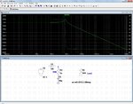
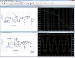
Capture1-1-2016-20.16.15.jpg
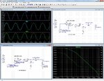
The actual circuit (as it should work) is figure (1). It tries to stabilise the AC current given to the grid (V4). That current is measured with the help of R2.
As you can see the circuit is not stable, it oscillates (figure (2)).

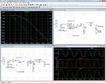
So I decided to measure the phase margin. This is done with the circuit from figure (3), by shortening any voltage source and adding an extra one in the feedback circuit. The result is hown in figure (4): a negative phase margin of 17 degrees, so 17 degrees past the oscillation point.

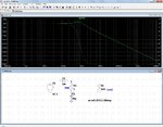
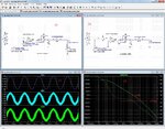
The oscillation can be stopped (or phase margin improved just enough) by connecting R3 across L1, but that will render L1 in my final project (its the purpose is to stop PWM switching signals in the direction of the grid) useless (besides the unacceptable dissipation in R3 once I scale up the voltages).
Capture1-1-2016-20.45.22.jpg
Also the impedance of the grid influences the phase margin, the lower the better, but that impedance if of course out of my control.
Increasing e.g. the grid impedance to 0.5 ohms (still a very reasonable low value), the instability is there again, even with R3 connected.


My questions are:
- Is my measuring method of the phase margin OK?
- If so, how to improve (a lot) the phase margin of the circuit shown in this post?


Thanks in advance!

Additionally I want (in some cases) the grid to be disconnected, and the control loop to act as an AC voltage stabilisation. In this case the results are even more disasterous, because now the PWM filter capacitor C1 is not almost shorted by the grid...
 
Last edited:

A second-order low pass has an asymptotic phase shift of 180 degree, a high Q filter reaches near to 180 degree above the cut-off frequency. A straightforward solution is to tune the control loop for a transition frequency below the filter cut-off.

The option implemented in your example, adding a zero to the filter characteristic, does basically work. It's often utilizing filter capacitor ESR or an added series resistor. Finally, a stable current control can be better implemented with the current sensor on the left side of the filter.

Feedback loops involving PWM filters are always compromise solutions, they can't achieve perfect characteristics.
 
  • Like
Reactions: DanyR

    DanyR

    Points: 2
    Helpful Answer Positive Rating
Thanks so much.
I did some measurements about an LC circuit only (no amplification or feedback), only with a "load" resistor across the C, and I saw the phase jumping indeed from 0 degrees to 180 degrees at the resonance frequency. Of course (as you stated) this will always give problems in a closed loop system: one can not get the phase margin above zero degrees.
Again, as you said, adding a series resistor to the C limits the phase jump to 90 degrees, giving some chance of an acceptable phase margin in a closed loop system.

No series resistor: 180 degrees phase shift
Capture4-1-2016-20.06.12.jpg

With series resistor: 90 degrees phase shift
Capture4-1-2016-20.06.28.jpg
I see that the minimal value of the series R is the C impedance at the resonance frequency to make the phase swing max 90 degrees.


Finally, a stable current control can be better implemented with the current sensor on the left side of the filter.
The problem is then that I also measure the current through the capacitor (at PWM frequency), and I wanted purely the 50 Hz current through the load. Any suggestions how to solve this?
 
Last edited:

Hi, I think my problem still exists.
Adding a resistor in series with the filter capacitor C1 improves the phase margin a lot, but still the latter is only slightly above zero (due to the phase shift of 90 degr. in the filter and another 90 degr. in the op-amp I assume). The minimal resistor I have to add is 4 ohms, with a lesser value the circuit oscillates, and a higher value does not improve the phase margin any more.

Capture8-1-2016-12.42.01.jpg

Any suggestions?
How is this done in commercial grid tied invertors?

Thanks in advance!
 

Tuning the control loop also involves modifying the error amplifier gain. 90 degree error amplifier phase shift at the loop transition frequency shouldn't be taken as granted. There are possible means like lead-lag compensation.
 
  • Like
Reactions: DanyR

    DanyR

    Points: 2
    Helpful Answer Positive Rating
Tuning the control loop also involves modifying the error amplifier gain. 90 degree error amplifier phase shift at the loop transition frequency shouldn't be taken as granted. There are possible means like lead-lag compensation.
Hi FvM, thanks for your answer.
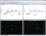
I did a simulation with a (very much, factor 1000) lower open loop gain (by changing the formula of B1, resultin in a 1000 times less voltage), and was able to achieve a phase margin of approx 40 degrees, even without series resistance of the filter capacitor.
The only drawback now is that the output current is slightly out of phase with the input voltage. Probably the gain has become too low now to correct that. I have to figure that out.

Capture9-1-2016-20.37.14.jpg

I did try to undertstand also the lead and lag compensators but the documents handling them are not very clear (at least to me...). Anyway, if I can achieve enough phase margin by reducing the open loop gain that is good enough for me! :-D
 

Danny, this problem is pretty much insoluble because there is no way of knowing what type of wildly changing reactive and resistive load is going to be connected to the output of your inverter.

The output is "wild" in both amplitude and phase, and there is no way to design some kind of phase compensation network to correct for that.

There are a couple of approaches to amplitude control of a PWM inverter.
The first is the classic class D amplifier where the output switched waveform itself is used to generate the PWM, and the output LPF (and reactive load) are external to the control loop.

This is not as successful with an inverter as with an audio power amplifier because of the highly variable and unknown load, but it may be good enough for the purpose.

For software generated PWM, all you need to know is the final output amplitude after the filter. Phase does not come into it. If the peak output voltage is correct, job done.
If its not, switching to a different a different PWM lookup table, or other software trick steps the amplitude up or down a notch. That is probably the best method, but there may still be some half cycle surges and sags during sudden step load changes.
 
  • Like
Reactions: DanyR

    DanyR

    Points: 2
    Helpful Answer Positive Rating
Hi Tony, thanks for your elaborate reply.

Danny, this problem is pretty much insoluble because there is no way of knowing what type of wildly changing reactive and resistive load is going to be connected to the output of your inverter.
The output is "wild" in both amplitude and phase, and there is no way to design some kind of phase compensation network to correct for that.
I think the output is not so "wild".
Either (1st possibility) the output is connected to the grid, which has a very low internal impedance (resistive/inductive) as shown in my simulations,
or (2nd possibility): the output is not connected (open). The latter case is not present in my simulations (yet).

So, for stability measurements I have a "load" of e.g. 1 ohm resistive in series with 1 ohm inductive maximum. The minimum value is (theoretically) zero.

There are a couple of approaches to amplitude control of a PWM inverter.
The first is the classic class D amplifier where the output switched waveform itself is used to generate the PWM, and the output LPF (and reactive load) are external to the control loop.
Yes, that is what I wanted to do. Currently I try to figure out what the control stability of the whole circuit would be when adding the LC PWM output filter (see https://www.edaboard.com/threads/346709/).

This is not as successful with an inverter as with an audio power amplifier because of the highly variable and unknown load, but it may be good enough for the purpose.

For software generated PWM, all you need to know is the final output amplitude after the filter. Phase does not come into it. If the peak output voltage is correct, job done.
If its not, switching to a different a different PWM lookup table, or other software trick steps the amplitude up or down a notch. That is probably the best method, but there may still be some half cycle surges and sags during sudden step load changes.
What I do is trying to stabilise the output current, not the voltage. The latter one is fixed (equal to the grid voltage). See the first post, figure 1. Of course I try to make the output current to be in phase with the grid voltage (not shown in the simulation, but see https://www.edaboard.com/threads/346709/ again.
Only if the output is not connected to the grid I try to stabilise the output voltage (not simulated here).
 

What I do is trying to stabilise the output current, not the voltage.
But you have to do it by controlling a voltage, the output of your PWM stage. Trying it in a simple control loop brings up the previously reported problems.

There are different approaches to solve it in a more complex controller topology. You can e.g. implement a combination of voltage feedforward and current feedback. In the forward path, you predict the required inverter output voltage including the voltage drop at the series inductor. Current feedback is reducing residual errors.

The current feedback controller may also use "rotating" I-Q coordinates, allowing exact and independent control of real and reactive current for the fundamental.
 
  • Like
Reactions: DanyR

    DanyR

    Points: 2
    Helpful Answer Positive Rating
It depends if the output is current fed or voltage fed.
I have never seen a current fed general purpose (open output) inverter, but for grid tie operation, current fed output should offer some definite control advantages.

I doubt if its possible to design a universal circuit topology that can serve both grid tie and open output applications, the two are so completely different.
 
  • Like
Reactions: DanyR

    DanyR

    Points: 2
    Helpful Answer Positive Rating
It certainly is a solvable problem, but I feel that the OP is quite new to control theory. DanyR, you should review documents on lead lag compensation, and familiarize yourself with type I, II, and III error amplifiers. Personally I recommend reading the white papers from Venable (it asks you to give your contact info, feed it garbage if you want), they are quite readable.

FvM brings up the excellent point of using a rotating reference frame for control (aka cartesian feedback). This works very well when synthesizing sinewaves, since a sinewave has zero bandwidth, regardless of its frequency. Though this requires knowing how to use frequency mixers, or a microcontroller, it's basically the ideal solution so long as your output needs to be sinusoidal (and your load is linear!).
 
  • Like
Reactions: DanyR

    DanyR

    Points: 2
    Helpful Answer Positive Rating
Thanks for the replies! :smile:

It certainly is a solvable problem, but I feel that the OP is quite new to control theory.
Yes, indeed, I am new to control theory.

DanyR, you should review documents on lead lag compensation, and familiarize yourself with type I, II, and III error amplifiers. Personally I recommend reading the white papers from Venable (it asks you to give your contact info, feed it garbage if you want), they are quite readable.
Thanks for the link. I have downloaded all documents and will have a look into them.

FvM brings up the excellent point of using a rotating reference frame for control (aka cartesian feedback). This works very well when synthesizing sinewaves, since a sinewave has zero bandwidth, regardless of its frequency. Though this requires knowing how to use frequency mixers, or a microcontroller, it's basically the ideal solution so long as your output needs to be sinusoidal (and your load is linear!).
Hm. Most of what is said in above quote I do not know/understand yet. I will try to find some documentation.
 

Hi, the white papers from Venable indeed helped me a lot, especially the one called "03-Technical-Paper-Optimum-Feedback-Amplifier-Design-For-Control-Systems".
The only thing I had to add to the control loop in my simulation was a type 2 error amplifier in stead of a simple one.

This is the result:
Capture18-1-2016-18.49.32.jpg
It shows there is a phase margin of approx. 50 degrees, which is Ok I think.

The "frequencies" of the error amplifier are:
UGF: 1083 Hz
Zero: 531 Hz
Pole: 1659 Hz. see the definitions in the Venable document above.

The phase margin is much better than in the method of decreasing gain (post #6), even with the ESR of the filter capacitor removed and an inductor added to the grid impedance.

But: I see that the overall open loop gain at 50Hz is only 20 dB, what is roughly the same as the one in post #6 (the one with decreased gain). 20 dB is not very much (10 times).
Also the small phase error between the output current and the reference voltage is there (same as the one in post #6), and additionally the output current has not the same "value" (left alone the units) as the reference voltage. The latter is caused by the type 2 error amplifier nature.

I will try to make the whole loop to have a better open loop gain at 50Hz, preserving the phase margin of above circuit.

Thanks all again for your replies! They helped me a lot! :grin:

Added: I see I have used a deviating filter capacity in the AC analysis test (it should be 40uF instead of 4uF). The results/conclusions stay however roughly the same.
 
Last edited:

Status
Not open for further replies.

Part and Inventory Search

Welcome to EDABoard.com

Sponsor

Back
Top