Continue to Site

Welcome to EDAboard.com

Welcome to our site! EDAboard.com is an international Electronics Discussion Forum focused on EDA software, circuits, schematics, books, theory, papers, asic, pld, 8051, DSP, Network, RF, Analog Design, PCB, Service Manuals... and a whole lot more! To participate you need to register. Registration is free. Click here to register now.

[SOLVED] [Moved]: Do I need to make a DC path at the input of an op amp?

Status
Not open for further replies.

matrixon

Junior Member level 1
Joined
Dec 1, 2014
Messages
19
Helped
0
Reputation
0
Reaction score
0
Trophy points
1
Visit site
Activity points
151
I've heard that a DC path is needed
at the input of an op amp,or the op amp
won't be functional because there is no
path for the input bias current.
(in the image below,R1 provides a dc
path for input bias current)
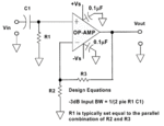
C0248-Figure2.gif

But if I use MOSFETs to design an op amp,is there still input bias current(the gate of MOSFETs have no current)?Or do I still need to add R1 to make op amp functional?
 

Re: Do I need to make a DC path at the input of an op amp?

R1 will still be needed with a jfet op amp to keep the input voltage within the input common mode range. Without R1 the input voltage to the op amp could drift up and down randomly depending on the voltage charge on C1.

There really always needs to be a dc path, the problem could be due to bias current with bipolar op amps, or with fet inputs, a randomly wandering input voltage.

why the input voltage to the op amp could drift up and down randomly?
there is no current flow into the gate of a MOSFET,the gate voltage is independent to current,why C1 can be charged?
 

You need a ground reference to establish the voltage at the MOSFET input, otherwise stray charges can cause it to go a random value.
Also MOSFET inputs often have a diode connected to V- and/or V+ for overvoltage protection and there will be some leakage current through them that requires a path to ground.
If you look at the data sheet for a MOSFET op amp it will list the input bias current (which although very small, is still finite).
 

You need a ground reference to establish the voltage at the MOSFET input, otherwise stray charges can cause it to go a random value.
Also MOSFET inputs often have a diode connected to V- and/or V+ for overvoltage protection and there will be some leakage current through them that requires a path to ground.

But if I design the input stage without diode connected,the input
can be model as an open (as T model expresses),there is no
cap or resister to ground at the input to let stray charge estabilish
a voltage at input .
 

The general advice about IC's applies here: Do not leave any input floating, or else it is subject to influence by EMI or ambient mains fields. Tie it to a stable voltage source, through sufficiently high or low resistance that allows it to operate.

An exception to the rule is if it has an internal connection to a stable voltage source.

Mosfets have an extremely high input impedance, making them more prone to misbehave even than transistors.

An input capacitor (C1 in post #1) causes sort of a gray area in this regard. Nevertheless it still leaves the input at high impedance, free to wander up or down in terms of DC level. That is one reason to keep R1.

Another reason is that R1, with the capacitor, creates a filter. The caption refers to this.
 
You are really persistent in claiming that a MOSFET OP has no input current.

Technically, this is simply wrong. Any MOSFET has a certain leakage current, every technical IC is designed with protection diodes, etc. You'll refer to datasheest of real OPs to know the actual input current. It's at least some pA at usual ambient temperatures for general purpose OPs, down to fA for special "electrometer" OPs.

But assuming an ideal OP (and also ideal capacitor) with no input current doesn't solve the problem. It still leaves the voltage at the OP input node undetermined. You'll need a switch to charge the capacitor to a known voltage when starting circuit operation. If you have reason to presume zero charge of the capacitor (zero volts across it), you can simply replace the capacitor by a short, the other simple solution for your problem.

Either the series capacitor is part of a DC-blocking high-pass, then it needs a supplementing shunt resistor, or it's useless and can be omitted.
 
Even the capacitor itself will have some small leakage.
There's no such thing as infinite resistance in the real world.
And as FvM noted, if the capacitor is looking into an open circuit then it has no purpose.

But if we still haven't convinced you that you need a DC path then go ahead and build the circuit without one, just don't say we didn't warn you of the consequences. ;-)
 
Having a high impedance and input current input load is good for low input offset voltage amplified by high gain.
Ensure you calculate this effect in any choice of input DC termination to a reference voltage , be that 0 or V/2.

Also allow for leakage effects from dust and moisture , which can often be << 10M in forced air environments and increase with time unless in a hermetic sealed environment.

Also allow for capacitive ingress from pulse noise and accumulation of voltage from this effect of input capacitance by having a "bleeder" resistance to the preferred voltage reference such that Vin (+) - Vin(-) = 0 at all times for linear operation.

Best practice is to match input source resistance so that input bias currents, no matter how small are neutralized and then input offset currents * R source is added to Vio.

Got it?
 

Having a high impedance and input current input load is good for low input offset voltage amplified by high gain.
Ensure you calculate this effect in any choice of input DC termination to a reference voltage , be that 0 or V/2.

Also allow for leakage effects from dust and moisture , which can often be << 10M in forced air environments and increase with time unless in a hermetic sealed environment.

Got it?

So dust and moisture can be model as a very large resistor to gnd, input current can be viewed as flowing through it and produce a large voltage change at input terminal?
 

Re: Do I need to make a DC path at the input of an op amp?

why the input voltage to the op amp could drift up and down randomly?
there is no current flow into the gate of a MOSFET,the gate voltage is independent to current,why C1 can be charged?

Because...

"In theory, there is no difference between theory and
practice. In practice, there is".

Professors and textbooks live for idealizing assumptions.
Engineers have to deal with those lies and half truths.
 
The mistake a number of people make is thinking that an open circuit/unconnected input from of an opamp is zero volt.

Floating inpit/Open circuit doesn't imply zero volt.

In practice, without the pulldown resistor, a number of factors will contribute toward the voltage on that node: crosstalk, EMI, Rf pickup... Good idea is to have the resistor in place, and in fact the lower it is, the higher the noise rejection, but of course not too low to overload whatever source is driving the opamp
 

So dust and moisture can be model as a very large resistor to gnd, input current can be viewed as flowing through it and produce a large voltage change at input terminal?

Yes. If you have a differential leakage resistance on one input path of 10 MOhm and 10nA input bias , this would create an input offset voltage of 0.1V times the gain. for the output.
Obviosly depending on corrosive solder flux residue, moisture content and dust, you can expect a wide range of leakage resistance between exposed conductors.

So exposed copper area should be minimized and conformal coating considered for harsh environments.
iPads & Laptops generally stop working from rust when any rain gets inside due to contaminants, mild corrosive flux ( like no-clean) and dust. ( perhaps by design ) but could be improved greatly
 

Status
Not open for further replies.

Part and Inventory Search

Welcome to EDABoard.com

Sponsor

Back
Top