Continue to Site

Welcome to EDAboard.com

Welcome to our site! EDAboard.com is an international Electronics Discussion Forum focused on EDA software, circuits, schematics, books, theory, papers, asic, pld, 8051, DSP, Network, RF, Analog Design, PCB, Service Manuals... and a whole lot more! To participate you need to register. Registration is free. Click here to register now.

Broad-band Impedance Matching Problem.

Status
Not open for further replies.

cannibol_90

Member level 5
Member level 5
Joined
Jun 20, 2009
Messages
83
Helped
5
Reputation
10
Reaction score
5
Trophy points
1,288
Visit site
Activity points
2,066
Is it possible to match a 500 KOhm output to a 50 Ohm load over a broad frequency range of 0.5 - 7 GHz?
 

its looks impossible to me since the Qmax to meet the bandwidth (6.5GHz) is 0.097.
 

hi,
matching can be done using a shunt resistor. however the this matching network will incur high loss. lumped element matching is preferred but matching 500kOhm with 50ohm is impossible using lumped element.
 

Matching 500k at 6 GHz sounds like a completely absurd idea.

Can you briefly tell about the actual design problem?
 

OK! Now that I have drawn your attention, let me explain. :wink:

I had posted this problem earlier in the following post: https://www.edaboard.com/threads/343243/.

1. We have a Ring VCO which outputs for a high port impedance of 50 KOhm. At 50 Ohm the output is pulled towards the ground. The VCO has a tuning range from 0.5-6.5 GHz. We want the output to be matched to a 50 Ohm port. How can we achieve this?

2. The flicker noise (noise at low frequencies) appears too high. What must be the change in the noise parameters so that the flicker noise is reduced? We used +NLEV = 2, EF = 0.907, AF = 0.9065, KF = 8.704E-29 for NMOS and +NLEV = 2 EF = 1.152 AF = 1.052 KF = 8.262E-28 for PMOS. We are attaching the schematic of the circuit with its phase noise plot.

vco.jpg PN.jpg
 
Last edited:

All I can think of is a broadband buffer. MMIC, source follower or a combination. Can't say what that may do to the noise figure.
 
I had posted this problem earlier in the following post: Adaptation of a 50Ω Port to a CMOS Ring Oscillator in AWR AO.

You already got the suggestion to buffer the RO output in your previous thread. For some reason, you seemed to ignore it until now.

Impedance matching is the wrong topic here. You don't want to achieve maximum power transfer. Instead you want to use a "high impedance" buffer between the oscillator and the output. The buffer will still add some capacitive load to the oscillator, but keep it almost undisturbed.
 

    V

    Points: 2
    Helpful Answer Positive Rating
Thanks FvM and ydtech for your replies!

I get it, like an Op-amp, or a common drain amplifier! Am I right? These have high input impedance and low output impedance. But isn't the power gain high for a common drain amplifier? This will lead to a high power dissipation, isn't it?

Can you please help me know some buffer amplifier circuits suitable for this Ring Oscillator configuration for low power dissipation?

Kindly help us.
 
Last edited:

dear cannibal,
I'm not really an expert in ring oscillators, but have designed colpitts and hartley oscillators before. Why don't you try hartley oscillators? Hartley generally wideband oscillators. Will it give the bandwidth you wanted? The reason is because the output impedance of hartley will be reasonable and you can design a buffer to get high gain at the output.
 
Thanks pragash for your reply! We are not encouraged to design Hartley or Colpitts oscillator. The power consumed must be very low.

What kind of a buffer can help us in implementing a high input impedance, low output impedance, low power consuming circuit?
 

We seem to get this sort of question a lot. "I have a nice VCO which simulates very well until I put a load on it, help." This is normal for VCO of various types, their performance is greatly affected by loading at the output. So you want a buffer at the output. At >1GHz you best bet is to use an inverter cascade with proper biasing (common mode feedback). And make sure your output has DC blocking before the output port.
 
mtweig, can you please provide us with a simple circuit diagram of "cascaded inverter with common mode feedback". All that comes into our mind is NMOS and PMOS tied to form an inverter and cascaded. What is the common mode feedback in inverters? We are working on MOSFET/VLSI circuits for the very first time. Of course, we googled for it; found some thesis and papers. But, none of them explains the design part nor provides a proper circuit.

An excerpt from RF Components and Circuits by Joseph J carr: "An emitter follower is also frequently used as a buffer amplifier, which is an intermediate stage used to isolate two circuits from each other. One example of this is in the output circuit of oscillator circuits. Many oscillators will pull or change the frequency if the load impedance changes. Yet some of the very circuits used with oscillators naturally provide changing impedance situation. The oscillator proves a lot more stable under these conditions if an emitter follower buffer amplifier is used between its output and its load."

I believe the situation of changing impedance occurs when the current through the load changes, which varies the gm and hence the output resistance. So a common drain amplifier as a buffer can't maintain a steady output impedance of 50 Ohms?
 
Last edited:

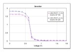
As a start, we implemented a basic CMOS inverter for a 50 Ohm output port impedance. We used a common drain buffer amplifier for matching purposes. But, the width of the buffer had to be increased to impractical values. This was compared to an inverter response with a high output port impedance of 50 MOhm. Figure below shows the schematic of an inverter with its voltage characteristics. The problem being, common drain with an output port impedance of 50 Ohm consumes high power of about 58 mW, while with a high output impedance consumes a mere 6.55e-5 mW.

Inverter.jpg inverter response.jpg
 

Sounds like you are complaining about ohms law. Driving e.g. 10 mA into a 50 ohm load involves 18 mW power consumption from the 1.8V node.

You may want to specify what's your required 50 ohm output. Then design the buffer + optional output attenuator respectively.
 

mtweig and FvM, can you please provide us with a simple circuit diagram of "cascaded inverter with common mode feedback"?
 

Status
Not open for further replies.

Similar threads

Part and Inventory Search

Welcome to EDABoard.com

Sponsor

Back
Top