Continue to Site

Welcome to EDAboard.com

Welcome to our site! EDAboard.com is an international Electronics Discussion Forum focused on EDA software, circuits, schematics, books, theory, papers, asic, pld, 8051, DSP, Network, RF, Analog Design, PCB, Service Manuals... and a whole lot more! To participate you need to register. Registration is free. Click here to register now.

doubts in circuit diagram of LPC2148

Status
Not open for further replies.

embpic

Advanced Member level 3
Joined
May 29, 2013
Messages
742
Helped
80
Reputation
160
Reaction score
77
Trophy points
1,308
Location
india
Visit site
Activity points
5,213
hello master's
i am using lpc2148 and using arm dev. board but i need to design for my project. and i have some doubts in design as follows.

1. I want to use supply which is optional whether to from USB or +5v DC power supply from wall socket.
2. if I connect vcc of USB to Vcc of Power supply and I am using both USB and external power supply then will it harmful to PC?
or I have to keep it isolated from each other.
3. how to include ISP & J-TAG debugging (10-pin) for loading firmware.
4. also thinking to add microSD in design.

i have attached circuit diagram which was got with dev board. and i am using it for core.
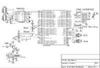
 

sir i have post a circuit of dev board which was in pdf and i need to design a new PCB for my projects. and i am giving to professional PCB designer.so i have theses doubts to design for me.
 

One power supply should not be allowed to contact the other power supply. You should use steering diodes, or a relay, or a 3-conductor auto-switch jack, etc.

If you could be sure the supplies would never be at uneven volt levels, it would theoretically be okay. However it is too risky to your expensive equipment.
 

It is difficult to provide an in-depth critic of your design due to the low resolution of the uploaded image.

However, there definitely seems to be a lack of the necessary bypass caps on the power lines of the LPC2148.


Why not save yourself some frustration and concern, by adapting one of the myriad of available schematics of known reliable design for a LPC2148 dev board?

For example:

Olimex LPC-P2148 Product Page

LPC-P2148 Schematic


Also checkout the NXP website as they typically offer extensive reference material on best practices for designs which utilize their products like the LPC2148.

Topics like bypass cap requirements, suggestion for crystal location, PCB design, etc, are typically covered in-depth.


BigDog
 

thank you sir,
i have uploaded pdf file which is got with dev. board and i have selected some part from that circuit.
like

power supply
power led
I2C eeprom
sd interface
and all from third box.

sir i refer some schematic and found that it is related and same with this one.

- - - Updated - - -

here i have attached pdf
 

Attachments

  • Dev_Board.pdf
    574.5 KB · Views: 128

Status
Not open for further replies.

Similar threads

Part and Inventory Search

Welcome to EDABoard.com

Sponsor

Back
Top