Continue to Site

Welcome to EDAboard.com

Welcome to our site! EDAboard.com is an international Electronics Discussion Forum focused on EDA software, circuits, schematics, books, theory, papers, asic, pld, 8051, DSP, Network, RF, Analog Design, PCB, Service Manuals... and a whole lot more! To participate you need to register. Registration is free. Click here to register now.

[SOLVED] Explain NMOS ID vs VDS curve graph

Status
Not open for further replies.

vleam13

Member level 1
Member level 1
Joined
Mar 3, 2010
Messages
37
Helped
1
Reputation
2
Reaction score
1
Trophy points
1,288
Visit site
Activity points
1,560
Hi,

I simulated NMOS characteristic and attached image is the results.
From the graph, looks like saturation happen after green line.
Theoretically, saturation shall happen when Vds>Vgs-vth (red line)

Anyone can explain this phenomena?

Thanks.


Attachments

  • Untitled.png
    Untitled.png
    24.1 KB · Views: 3,520

Re: NMOS ID vs VDS curve

tangent of green gives ON resistance or ESR of 1V/6mA=167 Ω
The Red load line looks like 780Ω so Gm looks better or transconductance value.

Is there a load resistance?
 

Re: NMOS ID vs VDS curve

tangent of green gives ON resistance or ESR of 1V/6mA=167 Ω
The Red load line looks like 780Ω so Gm looks better or transconductance value.

Is there a load resistance?


76_1339576062.png


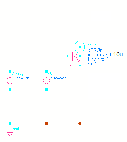
no load condition. Only simple simulation. Attached simulation circuit. Thanks.
 

Re: NMOS ID vs VDS curve

Yes. The transistor enters saturation only at red line points but the region between green and red lines is also considered as Active region or Triode Region of the transistor's operation.

All the best.

I agree with sunny too.

- - - Updated - - -

Yes. Its no load condition only. U got to see its model properties for further details on the transistor's behaviour.


Mean that triode region can be divided into two area with different Ron or Gm? I never read this in any book.......
 

Re: NMOS ID vs VDS curve

Actually ideal curves as per Vds>Vgs-Vth for saturation will be different from the one which u got.

They will keep increasing till the red line points and will become constant from there on.

Here they seem constant from green line points itself. Its because of varying model properties. A transistor in any model will be defined by some 90 plus properties.

- - - Updated - - -

The region between green line points and red line points is termed as "sub-threshold" region of operation.

It occurs just before entering the saturation region. This concept will be available in many VLSI text books.

Just refer to it.
 

Re: NMOS ID vs VDS curve

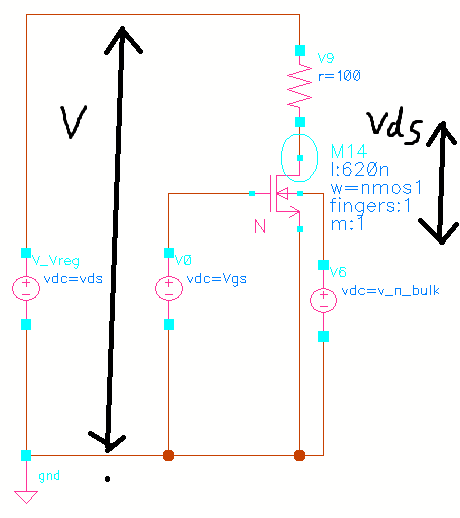
Test bench shown in #3 is not correctly simulated as Drain-Source voltage is not varying with Drain-source resistance. I mean is by this circuit you will see false region shown by red line. MOSFET comes in saturation from green line, because slope is very less shows device reached saturation.
To correct test-bench, add 10k resistance at the drain and then simulate.
 

Re: NMOS ID vs VDS curve

Is the Vth 0.7? The defualt value of Vth in spice model is 0.7, but mostly it wont be 0.7 in high technology node.
 

Re: NMOS ID vs VDS curve

Is the Vth 0.7? The defualt value of Vth in spice model is 0.7, but mostly it wont be 0.7 in high technology node.

Is around 0.8V.......

- - - Updated - - -

Test bench shown in #3 is not correctly simulated as Drain-Source voltage is not varying with Drain-source resistance. I mean is by this circuit you will see false region shown by red line. MOSFET comes in saturation from green line, because slope is very less shows device reached saturation.
To correct test-bench, add 10k resistance at the drain and then simulate.

Hi, Varunkan2k,

Could you explain more detail?
Why we need to put resistor? Voltage of ideal voltage source won't change and we want to make Vds vary with Id current?
Drain-Source resistance = Ron?

I have tried with 100ohm resistor (10K is causes big voltage drop across resistor and Vds is too small)
can't really see big different from my simulation without resistor.


71_1339643656.png


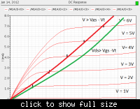
green line is estimated because neeed to consider voltage drop across resistorfor Vds
 

Re: NMOS ID vs VDS curve

First thing you need to know that, before going to test the behavior of device, the device should have been correctly biased.
So now, please make sure, device can carry the biased drain current. If you sweep the supply, MOSFET should not cross break down limits.
Now, please tell us, what is the drain current, what is the device width, and what is the drain-source resistance?
(to limit drain current use the appropriate load resistance)
Reason is, if you bias incorrectly, may be the device model you are using not correct.
Hope you understood my point.

Thanks for your reply.

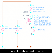
This nmos is 5V mos.
When both vds and vgs = 5V
Drain current is 5.6mA
width = 10um, length = 620nm,
drain source resistance for this condition = Vds/Ids = 791ohm....
I think MOSFET should not cross break down limit (vds around 7++ V) and working fine.
I feel that NMOS is biased in correct way. Please correct me if I am wrong.
Not really understand why trode and saturation region barrier different with ideal case.


Re: NMOS ID vs VDS curve

Ah, better you bias it with 10-100uA. and then check the response.
---
by the way, the shown MOSFET is 5V device, right? then it can't withstand 7V. Check the pdk please.
 
Last edited:

Re: NMOS ID vs VDS curve

Ah, better you bias it with 10-100uA. and then check the response.
---
by the way, the shown MOSFET is 5V device, right? then it can't withstand 7V. Check the pdk please.

Ya 5V device, but from the manual, mosfet will break down around 6.5V.
To bias nmos with 100u, I need very big drain resistor. I need to sweep input voltage to very large voltage (voltage drop across resistor is very big) so that vds is high enough for nmos to operate. It doesn't looks pratical for this testbench......

- - - Updated - - -

Actually ideal curves as per Vds>Vgs-Vth for saturation will be different from the one which u got.

They will keep increasing till the red line points and will become constant from there on.

Here they seem constant from green line points itself. Its because of varying model properties. A transistor in any model will be defined by some 90 plus properties.

- - - Updated - - -

The region between green line points and red line points is termed as "sub-threshold" region of operation.

It occurs just before entering the saturation region. This concept will be available in many VLSI text books.

Just refer to it.

Thanks for your information but sub-threshold is the region where Vgs < Vth but still conduct a little bit. So, that region is not sub-threshold region.
 
Re: NMOS ID vs VDS curve

It doesn't looks pratical for this testbench......
What is meant by this?
For the transistor size you used, 10um width, it can't handle more than hundreds of uA. So thats how the MOSFET works.
It should make the VDS zero.
Or if you want to fetch current of 1-10mA, Use MOSFET size of 10umX1000. and then try.
 

Re: NMOS ID vs VDS curve

Beta [uA/v^2] of the this nmos process > 2500 uA/V^2
and K > 0.55V^1/2
Id can goes up to 5mA when Vd = Vg = 5V for the size that selected.

What I can say on my simulation results now is green line is ideal and red line is non-ideal characteristic in my first post....

- - - Updated - - -

Dear all,

Thanks for the idea.
I tried using lower VG and VDS value and the I-V curve is very close to idea case where saturation happen when Vds > Vg -Vth.
I can make conclusion that "velocity Saturation" and "mobility degradation" happen when Vgs too high causes carriers to scatter against surface and reduce carrier mobility.

thanks.
 

Status
Not open for further replies.

Part and Inventory Search

Welcome to EDABoard.com

Sponsor

Back
Top