Continue to Site

Welcome to EDAboard.com

Welcome to our site! EDAboard.com is an international Electronics Discussion Forum focused on EDA software, circuits, schematics, books, theory, papers, asic, pld, 8051, DSP, Network, RF, Analog Design, PCB, Service Manuals... and a whole lot more! To participate you need to register. Registration is free. Click here to register now.

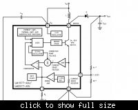
Node Analysis for LM2577 Block Diagram

Status
Not open for further replies.

HelloCthulhu

Newbie level 5
Newbie level 5
Joined
Mar 16, 2010
Messages
8
Helped
0
Reputation
0
Reaction score
0
Trophy points
1,281
Visit site
Activity points
1,357
Greetings Members

I'm a chemistry student doing some research [this is not homework!] on boost conversion and I need help discerning the node analysis for this step-up voltage regulator. I've found pretty decent tutorials on elements such as the comparator, npn transistor, and oscillator. But elements such as logic, current and thermal limit, undervoltage shutdown, soft start, driver stage, 1.23v ref., and the sigma symbol enclosed in a circle I can't seem to find any good tutorials on.

Basically I need help understanding how current flows inside of the LM2577. If anyone would be willing to educate me on this, I would be most grateful. Thank you!
 

Dear HelloCthulhu
Hi
I don't think there are any complicated thing ! but i'm a bit confused about what you need exactly ? do you need chemical analysis ( according thing that you told at your literature ! ) clarify , what do you need exactly thus , perhaps i can help you .
Best Wishes
Goldsmith
 

Thank you for the quick response!

I'm doing some experiments with boost conversion. I'm using a prefabbed LM2577 step-up voltage regular circuit to boost a 6v latern battery to 12v to power a 14w light bulb. But I don't fully understand how current flows inside of the LM2577. For example, after 6v flows through the 5 pin, it flows in a "2.5v regulator". I don't understand what happens to the current at this point. I also don't understand how current flows from the npn transistor, throught the "driver stage", to the "logic". These are elements of the circuit I can't find any information on, leaving my node analysis incomplete. I've added an image of the prefabbed LM2577 circuit I purchased. Any information you can provide would be most appreciated.


Pin 5, Vin, is only for powering the internal circuitry - it isn't used for the switching current. The switching current flows through the inductor then pin 4, then the NPN switch and the current sense resistor to ground (pin 3).

When the NPN transistor is turned off, the current flows from the inductor through the diode and into Cout/Vout

Keith.
 

Hi again
I think you didn't wrote the name of that IC correctly , isn't it ? i think it is LM2577 not LM2755 !!!? isn't it ?
Best Luck
Goldsmith
 

Thanks again for the response. It is LM2577.

---------- Post added at 20:10 ---------- Previous post was at 19:31 ----------

Thank you so much for your input, Keith.

I'm still a little confused regarding how current is flowing through the internal circuitry, so I hope it's alright if I go element by element with you. I'll be using a 6v lantern battery to power the circuit. What is happening to the current at Pin 5 at the "2.5v regulator" and how is current flowing to the capacitor [Cin]?

I greatly appreciate everyone's help with this. :-D
 

I wouldn't worry too much about how the internal circuitry is powered. The internal diagram is not complete - for example it doesn't show where the 2.5V goes. From a design point of view you only need to be concerned with the external components and a few key internal components/blocks such as the switching transistor.

Cin is a high frequency decoupling capacitor. It ensures that the high peak currents can be supplied to the inductor.

Keith
 

This is fantastic! I think I'm finally getting somewhere.

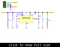
Ok, I'll explain what I'm working with. I'm trying to boost a 6v lantern battery to 12v to power a 14w light bulb. I'm using these elements as a template for learning more about how IC regulators and boost conversion work. Here's an image of the prefabricated boost converter I bought online:


I apologize in advance if I'm describing this circuit incorrectly. Let's assume that the 1kuF/63V capacitor is node 1,the 10k resistor is node 2, the left side of the 100uH inductor entering Pin 5 is node 3, the 100nF capacitor is node 4, and right side of the inductor entering Pin 4 is node 5. Basically, I'm trying to do the node analysis for this circuit with the npn switch closed first. How do I calculate the current as it flows from the 6v battery into each of the specified nodes as it enters and leaves the LM2577?

I greatly appreciate everything contributors to this thread have provided me. Thank you very much for all of your help.
 

Hi again
I think this formula can help you :
For boost converter we have this equation for out put amplitude : vout =vin/1-D.C which D.C in that is duty cycle ( pulse width ) .
Best Wishes
Goldsmith
 

When the NPN switch is closed the diode will be reverse biased so the only current flow will be from the input through the inductor, through the switch to ground. I am not sure what you are trying to calculate. The current through the inductor will initially be zero and will then increase with time, based on the inductance and the voltage across the inductor.

Keith
 

I've been gettting conflicting information regarding parallel rc circuit equations with a DC source. I feel like I'm getting nowhere :???:, so I think I'd better just ask the experts. Using a 6v lantern battery as the voltage source, how do I calculate the charging/discharging current at node 1 (1kuF/63v capacitor) and the current at node 2 (10kOhm resistor)?

I greatly appreciate your assistance! :-D
 

Status
Not open for further replies.

Similar threads

Part and Inventory Search

Welcome to EDABoard.com

Sponsor

Back
Top