shaikss
Full Member level 4

HI,
I am very confused how to connect my bulk of MOSes in my circuitary.
NMOS bulk should be connected to lower potential and PMOS bulk should be connected to higher potential of the system.
Moreover, Source and Drain are interchangeable and so whichever is at higher potential acts as drain. Guess I am correct at this statement.
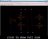
Now my question is: I have designed my rectifier circuit in which I have used cross coupled architecture of PMOS and NMOS.
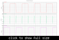
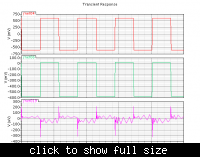
I have simulated and plotted the voltages of Drain, Source of NMOSes in order to finalise the bulk of NMOS.
Attached is the simulated result and schematic.
If at all, If I have used ground connection in my entire circuit, Can I connect the bulk of NMOS to grnd as gnd is at lower potential?
Please help me as I am in confused state.
Note: First and second attachement have three plots in each.
first plot is net connecting to +ve of V0
second plot is net connecting both drains of NMOS in accordance to symbol of NMOS.
Third plot is net connecting to -ve of V0.
In the schematic, for the first attachment of plots, I have grounded the bulks of NMOS and for the second attachment of plots, I have connected bulks to sources of NMOS in accordance to symbol of NMOS.
Please correct me.
