Continue to Site

Welcome to EDAboard.com

Welcome to our site! EDAboard.com is an international Electronics Discussion Forum focused on EDA software, circuits, schematics, books, theory, papers, asic, pld, 8051, DSP, Network, RF, Analog Design, PCB, Service Manuals... and a whole lot more! To participate you need to register. Registration is free. Click here to register now.

2.4 lna design narrow bandwidth

Status
Not open for further replies.

teawchoo

Newbie level 5
Newbie level 5
Joined
Oct 3, 2010
Messages
9
Helped
0
Reputation
0
Reaction score
0
Trophy points
1,281
Visit site
Activity points
1,349
Hi,

I am supposed to design a 2.4 GHz LNA and I don't know where to start, what topologies and what transistors to use in order to get very high gain. How to deal with impedance matching. I have really studied anything related to antenna transmission system before and having a very hard time getting started.

Any help would be very appreciated :)
 

You can use Avago ATF-36077, and there are some examples design in Avago website
 
  • Like
Reactions: TsokratesB

    TsokratesB

    Points: 2
    Helpful Answer Positive Rating
    V

    Points: 2
    Helpful Answer Positive Rating
Hi Teawchoo,

You also can use the SiGe HBT technology, for this range of frequency I have used BFP740 and BFP640, both with good results. I achieved 0.75 dB of noise figure with 18 dB gain at 2.4 GHz using the BFP740 from Infineon. Infineon also supplies you either s-parameters at different biasing condition or the Gummel-Poon non linear mode (which is independent of biasing. Only thing is that I do not recommend you to simulate NF with non linear models since some of them are no accurate). Adding a 4.7 to 12 ohms resistor in series with collector I also achieved unconditional stability from DC till 8 GHz. I found them quite easy to design and no problems, you will need to add some small track at emitters terminal (aka emitter degeneration).

Alternatively you have the pseudomorphic GaAs HEMT from NEC, they are robust with regards to P1dB but very difficult to stabilize at your first tentatives. I can recommend here the NE3510M04. Quite good as well.

If you have any circuit simulator you can use matching networks at input and output.

Good lucky, Enrico.
 

Thank you for the replies. I think I will be using a PHEMT, ATF-55143. And the topology I am thinking is two stage cascoding. However, I need to achieve a very high gain which is around 30 dB. Do you have any suggestions?
 

You should simulate two stages of ATF-55143, that is different from one stage design.
 

Hi, vfone,

One month ago, I designed a 10G LNA with 3 stages, the 2nd stage is a copy from the 1st stage, but I worry about the mismatch between stages, so I insert a isolator between 1st stage and 2nd stage. Because the LNA match conducted by microstrip line, and it's hard to simulate very accurately. Do you have any idea to design higher than 10G LNA without isolator?
 

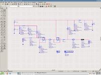
thank you so much i will simulate later but would something like this be okay?
 

Attachments

  • lna.jpg
    lna.jpg
    111 KB · Views: 211

30dB seems a very high gain requirement for an LNA stage... Why do you want this much gain?


If you really do need 30dB then why not design for 13dB gain with the ATF-55143 and then follow it with a 3dB attenuator (and maybe a band limiting filter?) and then a wide band 20dB gain block from MiniCircuits etc? This is more likely to be stable and will be less prone to out of band overload. I doubt you would get 30dB gain from your cascode circuit but I would expect the cascode to be unstable.

What NF and OIP3 do you need from the LNA?

If you need very high OIP3 then choose a gain block with high OIP3 (at the expense of high DC input power requirement)
 
Last edited:

If you really do need 30dB then why not design for 13dB gain with the ATF-55143 and then follow it with a 3dB attenuator (and maybe a band limiting filter?)
This 3 dB pad should influence LNA NF greatly, you can simulate the whole link budget and see the influence. You can use 3 stages, the 1st is low noise design, the 2nd is trade-off between noise and gain, the 3rd is OIP3 design.
 

For 2.4G, attenuator just a PAD, that is 3 resistors composite PI shape. You can simulate it in software to get insertion loss(attenuation) and S11. notice the resistor should be 0603 package.


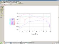
this is what i have and the simulation but the gain is stil not high enough.
 

If you need 30dB, you maybe need 3 stages.

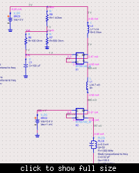
the 1st stage drain don't have Vdd voltage; and the 1st output why link to the Source of the 2nd?
 

im not sure how i am supposed to correct the 1st output and the source of the 2nd. how come the transistors have four connections instead of just g, d and s? Will 3 stages be more difficult if I were to build the board later?
 

1st just do one stage; then do more stage.
S1 can connect to S2 directly, they are both source. Sometimes link a conductance between gnd and source to increase stability. Just look for the datasheet of the transistor gate should be negative voltage, and Vd should be positive. Sometimes Avago use self-bias, so there is no need for negative for gate.
 
What is your specification for NF?

Also, your circuit modelling isn't suitable for use at 2.4GHz. You need to include the PCB substrate and model all PCB pads and via holes etc. Ideally this should be done with an EM simulator. I've designed several LNA stages using the 55143 and to get the best simulation I had to use an EM simulator. This gave a simulation that was remarkably close to the measured results. Failing this you could enter physical models for the PCB pads etc and use a simple linear simulator but this is not going to be as accurate unless you enter the models very carefully and there is negligible coupling between adjacent PCB pads etc.

I still don't think you will get sufficient gain from a cascode design. Also, you need higher voltage for it to operate. How will you bias the amplifier to have stable bias current and voltage over temperature? I always use the active bias network for the 55143 but I'm not sure how I would bias this device in cascode.
 
Last edited:

thank you for your suggestion i will use em simulator once I figure out what my circuit will look like at this point im just not sure what to do to get such a high gain. and I try to get low noise figure but the importance part is that it has to have high gain. I tried to look for examples but could not find anything
 

This 3 dB pad should influence LNA NF greatly, you can simulate the whole link budget and see the influence. You can use 3 stages, the 1st is low noise design, the 2nd is trade-off between noise and gain, the 3rd is OIP3 design.

It may not matter. It depends on the spec for the overall noise figure. The 55143 + pad + gain block may still meet the requirements. That's why it is useful to know the target NF. It could be 0.6dB, 1.0dB, 2.0dB etc....
 

So I started off again by setting a DC bias. How can I test the current gain from the amplifier?


Status
Not open for further replies.

Similar threads

Part and Inventory Search

Welcome to EDABoard.com

Sponsor

Back
Top